Continue to Site

Welcome to EDAboard.com

Welcome to our site! EDAboard.com is an international Electronics Discussion Forum focused on EDA software, circuits, schematics, books, theory, papers, asic, pld, 8051, DSP, Network, RF, Analog Design, PCB, Service Manuals... and a whole lot more! To participate you need to register. Registration is free. Click here to register now.

[SOLVED] About zero P_out for a voltage doubler rectifier in ADS

Status
Not open for further replies.

19127916

Newbie level 4
Joined
Apr 28, 2022
Messages
7
Helped
0
Reputation
0
Reaction score
0
Trophy points
1
Activity points
153
Hi,


I have designed a voltage doubler rectifier matched at 1.75 GHz.
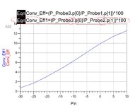
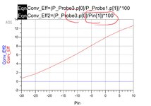
My problem is with HB simulation. I cannot understand what is the problem with my design that Pin and Pout are about zero and conversion efficiency vs Pin is negative nd zero.
I would be thankful if someone can help me to find the problem.

rect design.jpg

rect design s11.jpg
rect design conv P in and out all.jpg


Thanks
 

First you do multiple simulation simultaneously and it's very likely you confuse the datasets.( ADS will create a single dataset with simulation information with prefixes . Attention !!
Second, you have to add index number to Power Measurements like P_probe3.p[1]
Decrease the frequency step to able to see more precise.
Third, you circuit is working well around 1.75 GHz and you should change the HB frequency in according to.
Review you simulation set-up.
Hi,
Thanks a lot for taking the time to reply to my question.

1) In the uploaded image I just wanted to show all the simulation boxes, however, to run the HB simulation I disabled all the blocks except the HB and LSSP simulation to avoid any error.

2) Could you please let me know how I can add the index number?

3) The defined frequency of HB simulation is set to be 1.75 GHz and I tried different order numbers from 1 to 15, but did not get any better results.

I would be thankful if you can help me with these issues.

Thanks

ads1.jpg
 
Last edited by a moderator:

Doing LSSP Analysis is useless at this moment. Simply do your HB simulation and obtain a HB results only then compute your efficiency. Don't forget to assign 0 (zero) for frequency index while computing efficiency because you're interested in DC component of the output. So the Output Power must be Pout[0] the efficiency will be Pout[0]/Pin[1]
0: DC Component of the Output Waveform
1: Fundamental Input Frequency ( 1.75GHz for your case )
Thanks a lot for your answer.
Would you please advise me that how I can add the index?
 

Thanks a lot for your answer.
Would you please advise me that how I can add the index?
For instance ;
P_Probe3[0) syntax will give you DC Component of the Output.

P_Probe3[1] syntax gives you Fundamental Component, P_Probe3[2] will supply the Second Harmonic etc.
 
For instance ;
P_Probe3[0) syntax will give you DC Component of the Output.

P_Probe3[1] syntax gives you Fundamental Component, P_Probe3[2] will supply the Second Harmonic etc.
Thank you for your helpful answers.
I have applied your suggestion to the design. Now the efficiency is not zero anymore, but it is still very low.
How I can increase the efficiency to a value of about 40%?
 

Attachments

  • Eff_and_Vout_vs_Pin.jpg
    1.1 MB · Views: 131
  • Eff_vs_Rl.jpg
    909.1 KB · Views: 105

You measured The Power that Enters into the circuit. Check also Output DC Component over Available Power which is here Pin.
If there is a mismatch between the Source and the Circuit P_entered <<Pin due to mismatch. So you can see the efficiency of the matching circuit. This is the first part.
There will eventually be some other parameters but check that part first.
To my understanding, the Pin and the Power that enters into the matching circuit, P_probe1.p[1], should be the same.
As Pin is a variable in the design, if I define an equation like Efficiency=P_Probe3[0]/Pin[1], the resulting plot does not make sense.
However, if I rewrite the efficiency equation, considering P_probe3.p[0] as the output DC power and P_probe2.p[1] as the input power (which is in fact the output power of the matching circuit), I see no mismatch in the result.

Do you suggest any other way to check the mismatch?
 

Attachments

  • ads 2 eff.jpg
    ads 2 eff.jpg
    934.2 KB · Views: 101
  • ads 2 eff 2.jpg
    ads 2 eff 2.jpg
    945.2 KB · Views: 106
Last edited:

Pin is the Available Power from the Source and P_Probe1 measure the Power which enters into the circuit.
If your matching circuit is good, they should be equal. ( Ideal case )
P_Probe2 is the Power which is transferred into Diode Rectifier.
In order to see the overall efficiency, you can compare these powers and find where the power is lost.

All you have to do first, you have to find the Large Signal Input Impedance of the circuit with a LSSP simulation setup in a different schematic. For more information, pursuit the help. You can do this simulation with a HB analysis. You excite the circuit without matching components and measure the current and the voltage the divide voltage over current.
--- Updated ---

I simulated your circuit on a simplified set-up and I see that the Diodes' model is either limited or those diodes are not appropriate for rectification purposes. As you can see, the Input Impedance of the Rectifier part is frequency dependent and eventually frequency dependent. This is normal but they are small signal Schottky Diodes and their aim is to Detect not rectify. I think you should re-consider your circuit and find appropriate diodes for this target.
Look at Efficiency curve, it's not continuous due to limitation of the model.
1652393956941.png

1652393979792.png
 
Last edited:

Status
Not open for further replies.

Part and Inventory Search

Welcome to EDABoard.com

Sponsor

Back
Top