Continue to Site

Welcome to EDAboard.com

Welcome to our site! EDAboard.com is an international Electronics Discussion Forum focused on EDA software, circuits, schematics, books, theory, papers, asic, pld, 8051, DSP, Network, RF, Analog Design, PCB, Service Manuals... and a whole lot more! To participate you need to register. Registration is free. Click here to register now.

8 transistor full adder

Status
Not open for further replies.

Fuzail Hussain

Newbie level 5
Joined
Mar 19, 2012
Messages
8
Helped
0
Reputation
0
Reaction score
0
Trophy points
1,281
Location
india
Activity points
1,352
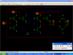
Iam trying to simulate 8 transistor fulladder circuit in DIGITAL SCHEMATIC.
If someone could check if the circuit is rightly constructed because it is not satisfing the logic of full adder
Picture4.png
Picture2.png
the circuit is designed in digital schematic and its paper diagram is also given

I don't find any fault in circuit construction but the output isn't satisfying the full adder truthtable.
Could anyone pls find out a solution.


Regards,

FUZAIL HUSSAIN S.
 

I don't find any fault in circuit construction but the output isn't satisfying the full adder truthtable.

Which combination goes wrong? The shown combination is correct: 1+1+1=11
 

Thank you for your reply .
the combination 1+0+1 and 1+1+0 isn't getting the result.I strongly find grounding might be error if you could design the circuit in DIGITAL SCHEMATIC and check for truth table then it would be appreciable as i think my design is faulty ....if not i would have got the ans.
Thank you again for your reply hope that you would solve it soon.
 

the combination 1+0+1 and 1+1+0 isn't getting the result.

You're right - at least partly. I think the 1+1+0=10 (1) combination gives the right result, even if the Cout output is only a "weak" logic 1.

The 1+0+1=10 combination, however, definitely goes wrong: Though the Sum output will get a correct "strong" logic 0 (if M3 is stronger than M1) (2), Cout = Cin · (A⨁B) + A·B (3) goes wrong, because the correctly created Cin·(A⨁B) weak logic 1 term is incorrectly overwritten (because the 2 terms must be ORed) by a (indeed correct transistor action and) logical correct A·B action which results in a strong logical 0 -- and so overwrites the weak logic 1 term -- the logical "OR" between these 2 terms fails.

So I think this circuit is not a correct full adder (4) -- at least not for this latter combination, because the logical "OR" doesn't work in this case.

(1) "+" here means (binary coded) arithmetic addition, not the logical "OR"
(2) numeration order from left bottom to top and then to right
(3) here, ⨁ means the logical EXOR, + the logical OR, · the logical AND
(4) even if some scientific papers claim this
 

Thanks again for being back soon.

I tried to figure out what you said but i couldn't get what you were explaining.However at the end you said the circuit might be wrong and i too think so.Also i would be thankful if you could give me the correct design as i took this as my project in my graduation course and i hav short time to submit.Also i found that for 1+0+1 combination during simulation in digital schematic both S and Cout were flickering(both were flashing on and off continously) neither single of them were on or off at given instant

I would love to understand your explaination why these above combinations went wrong but in simpler way('cause i couldn't understand what weak logic is... if weak logic corresponds to logic 0....then what does weak logic 1 in first line stands for....?)
Thank you
 

I tried to figure out what you said but i couldn't get what you were explaining.However at the end you said the circuit might be wrong and i too think so.
Sorry, I couldn't explain it better.

Also i would be thankful if you could give me the correct design as i took this as my project in my graduation course and i hav short time to submit.
Pls. understand that in the forum we shouldn't and we can't do your job. We just can try and help you to get it done. You can get help here for any reasonable question -- but we won't run your job.

Also i found that for 1+0+1 combination during simulation in digital schematic both S and Cout were flickering(both were flashing on and off continously) neither single of them were on or off at given instant
This shows that 2 different logic states with (rather) equal strength (s. below) fight against each other (it is called: "they clash" -- also called an output contention).

I would love to understand your explaination why these above combinations went wrong but in simpler way ('cause i couldn't understand what weak logic is... if weak logic corresponds to logic 0....then what does weak logic 1 in first line stands for....?)
Strong and weak logic drive states (sometimes also called "hard" resp. "soft") mean the drive strength of the respective logic state. Strong logic states overwrite soft logic states, i.e. the former win. You may imagine that a strong logic state results from a low series resistance, whereas a weak logic state has a large series resistance. So if you logically combine them, the strong logic level wins.

In your 1+0+1 combination Cout suffers such a clash: The first term from the realized equation Cout = Cin · (A⨁B) + A·B , i.e. Cin·(A⨁B) results in a correct logic 1 , but it is a weak 1 , because both S & G of M8 are logic 1, i.e. M8 is (nearly) closed, so can forward its S=logic 1 state to the drain only via a relatively large resistance -> that's why it is a weak logic 1 state.

Also, the second term AB -- provided by M7 -- indeed is created schematically and logically correct (A·B=0), and this is a strong logic 0 level, as the source (B) is a hard logic 0, the gate (A) a hard logic 1 , M7 fully open, so its drain provides a (correct) and strong logic 0 level. Now these 2 different logic outputs are combined (short circuited), and the stronger one (M7: AB=0) wins, so provides a logically wrong result in total. And why? Because the simple short circuit of 2 equally strong transistors doesn't provide the required OR function, but lets the stronger driving output win.

Solution? I'd say M8 must be much stronger than M7 , I'd estimate by a factor of 10.

You should know that this number-of-transistor-minimized full adder only works correctly at certain conditions:

  • appropriate VDD voltage for the individual process
  • appropriate W/L ratios for the individual transistors (PMOS always (much) larger than NMOS)
  • absolute PMOS & NMOS threshold voltages as close as possible

If you haven't already done so, study these papers thoroughly:

High Speed Low Power 8T Full Adder Cell with 45percent Improvement in Threshold Loss
A high Speed 8 Transistor Full Adder Design using Novel 3 Transistor XOR Gates

One of them even provides the individual W/L ratios for a 0.35µm process.

Good luck!
 
Last edited:
Whoa! that was helpful i found the error you were right it was hidden in M7and M8.Now all the combinations are being satisfied except for 1+0+1 its is showing 1+0+1=00 as output.
I understood that strong and weak logics ,also your explaination for for 1+0+1 i'll check out all the options you said.
The error i made was the M8 and M7 were in reversed (sideways)drain and source were interchanged.Now i made the correction by laterally changing them.

Thanks for your clue
 

Now all the combinations are being satisfied except for 1+0+1 its is showing 1+0+1=00 as output.
Try and make M8 about 10 times stronger than M7.

The error i made was the M8 and M7 were in reversed (sideways)drain and source were interchanged. Now i made the correction by laterally changing them.

In schematics -- if you don't use a 4-terminal symbol, i.e. with a separate bulk tap -- i.e. if you use a 3-terminal symbol, the bulk terminal internally (invisibly) is connected to the source, so source & drain aren't exchangeable.

In layout, however, this shouldn't matter, as source & drain of (integrated) MOSFETs are symmetrical and so are exchangeable. There's only one reason for a possible asymmetry: if the bulk tap (GND for nMOSFETs) is asymmetric in layout (which is mostly the case), it should be closer to the source than to the drain.
 

i tried m8 stronger by changin the aspect ratio W/L even 10 times but that had no effect 1+0+1 wasn't responding.......anything else shall i try.....?
well thanx for ur replis they did help me understand abt mosfets hope you would be responding d same way.......
i hav some thing to ask...also
i wanna do my masters in VLSI wat prior knowledge of electronics is essential if u could tell some topics 2 refer to get thorough understandin.....n help in my masters.........
 

i tried m8 stronger by changin the aspect ratio W/L even 10 times but that had no effect 1+0+1 wasn't responding.......anything else shall i try.....?

Did you try the W/L ratios of the "A high Speed 8 Transistor Full Adder Design using Novel 3 Transistor XOR Gates" paper, p.5?
 

yes i did the one recommended there....i changed w/l to 5:1 no response to that 1+0+1 input
 

haiii this is vamsi doing 9t full adder in sub threshold region could u please help me out in completing the project
 

atually i have tried it in tanner tools for proposed 9t full adder circuit and got the result but i dnt know how to cluclte the power clucations and i want extensin prjct of it can u help me in that hw to know the powe cucations i tried it with .power but it s giving wrong :razz: plese do help me cmplete the project i shud sbmit by may 6 th
 

I'd recommend analysis by simulation. Run a DC analysis for each of the 8 input patterns and measure the current drain from both the power supply and the input(s). Get the power consumption by multiplication of the individual input currents with their driving voltages and add all of them. From the results you can calculate an average and a maximum static power consumption.

To get dynamic power consumption, use a repeating sequence for the 8 input patterns (e.g. from a 3bit-counter), run ac simulations vs. the frequency range you need, and perform similar measurements and calculations.
 
actually boss s please dont mind in helping me i dont have that sound knowledge in those softwares as i was working and i have not attended my college everyday so please if u can solve the project i will be very thank full to u and giv me fb id this is my fb id krishnavamsi83@yahoo.com so that i can ge cope up with you and sorry for asking you lik this
 

Sorry, no - we don't run your job here in the forum - we are here to help you to run it yourself. Ask a concrete question, and you surely will get help!
 

Status
Not open for further replies.

Similar threads

Part and Inventory Search

Welcome to EDABoard.com

Sponsor

Back
Top