Continue to Site

Welcome to EDAboard.com

Welcome to our site! EDAboard.com is an international Electronics Discussion Forum focused on EDA software, circuits, schematics, books, theory, papers, asic, pld, 8051, DSP, Network, RF, Analog Design, PCB, Service Manuals... and a whole lot more! To participate you need to register. Registration is free. Click here to register now.

[SOLVED] 7 Segment 5 Digit Driver

Status
Not open for further replies.
Thanks for information @SunnySkyGuy,

But, i could not reach the point that i am trouble with the brightness of any led. I can not drive IC's properly and i don't know why. Opamp outputs behave strange than the first form of the circuit that i mentioned above, Why ?

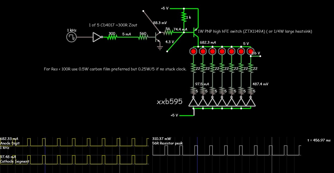
My opamp configuration is that inverting input is connected to 3.3V/2 by two 5.6k resistor divider network, non-inverting input of the opamps are connected to msp pins. Outputs of the opamps are inputs of the TC4017 and TPIC5b695 which are SER_IN,RCK,SRCK--- CLK and RST.

What is my mistake ? I don't really understand :(
 

EDIT: Where is the full schematic? Are these CC or CA digits?

I see tpic6b595 is used which is a 5Ω SIPO open drain driver > what is this for? It can only drive 0.5A with 2.5V drop then 2.3V drop for a good LED leaves only 0.2V drop for saturated switch and Rs !!!

Digit drivers must not have any resistors. I suggest 10mA avg per segment and thus 70mA avg per digit or 700mA per pulse on the Digit driver. The base current myst be 10~20% of the collector current unless Darlingtons or MOSFETS are used.

Only the segments have current limiting R's . Use Ohm's Law after all ESR voltage drops of drivers are considered and Vf of LED at rated current to calc ,. Segment R. e.g 2.5V for Red ( check spec) 1.2V for typ PNP Darlington Digit driver , 0.5V for Segment driver leaves 5-2.5-1.2-0.5=0.7V for 70mA, Rs=0.7V/0.07A= 10Ω

Digit voltage driver must drop depending on number of segments active.


Can you sketch a complete schematic with measurements for on/off for each stage and Vcc.
 
Last edited:

You have previously told about using "TL274" OPs, which isn't a known OP type for me. Did you mean TLC274?

I already mentioned that the OP level converter has problems to work at higher clock speeds, but I presume you are testing it with static logic levels now?
 

Yes, they are TLC274 opamps. I've tested in static conditions. For example, in the beginning i pause the code while rst pin of TC4017 high and measure the pins. Q0 never go high !

I've connect the output of the opamp which goes to TC4017 RST pin into the other breadboard and measured it. It was 5.0V but while i connect it again to TC4017 RST input it goes low to 3.98V :S In the datasheet, when the supply voltage of TC4017 is +5V high input offset voltage is 3.5V but if it is given to 3.98 to RST pin Q0 never goes high. So TC4017 do not work properly.

@SunnySkyGuy, i've posted my circuit without opamp connections in other post you can see it (post #32)

- - - Updated - - -

My application is at very low speed. Max speed of mux is 125Hz (8ms) that is not problem for TLC274 i guess. But, the general problem still can not be solved.
 

Yes 125 Hz, or even 50 kHz won't be a problem for TLC274.

No explanation for your observations so far, except for
- OP isn't TLC274
- counter isn't TC4017 (you have the printing perfectly hidden in your photo)
- one or the other is defective
- connection faulty (but looks correct in the photo)
- power supply problem
 

The actual circuit have 2 TLC274
Counter is TC4017 but in the picture i drawn it CD4017 it is not problem
Connection is correct i tested.
TLC274 power is +5.7V and TC4017 and TPIC5b's are +5V(because if i supply TLC274 with +5V outputs are approx. 4.3V)


I've tested TC4017 outputs while RST=0 give CLK=1 and 0 and again and again, none of the outputs of the IC goes high. Every measurement shows 0.01V or 0.05V max :S

I will try different IC :S for example CD4017 same but different manufacturer.

- - - Updated - - -

I've solved the 4017 problem by replacing TC4017 with CD4017BE. TC4017 does not work properly idk. Now,new problem is that while i am giving 0x00 off each display, segment A is always on also(for each digit), i can realize the mux operation my own eyes even the interrupt time 2ms or below(by assigning lower values to timer base i.e not 5000 instead 1000 or 500).

Please examine my last code and give me advice.

Thanks in advance.
 

@SunnySkyGuy, i've posted my circuit without opamp connections in other post you can see it (post #32)

ok then where is the Op Amp?

Your driver design is inverted.. the b595's 5 OHm drivers are for Common Cathode (CC) LED digits, NOT Common Anode (CA)
oops.

All CD4017's are pretty much the same with 200~350+ Ohm output impedance at 5V. You dont have enough drive and will need PNP after the NPN. both inverting to get a non-inverting Digit driver that can handle 700mA or so. Very detailed Ohm's Law Calculations.
 

According to your code
Code:
if((byte & mask)==1){
               SER_IN_h;
            }
            else if ((byte & mask)==0){
               SER_IN_l;
            }

if byte and mask are both 0x80 then result is 0x80 but you are only testing if result is 1.

So try this.

Code:
if(byte & mask){
               SER_IN_h;
            }
            else {
               SER_IN_l;
            }
 

@actor23< AS I indicated before , you have the wrong LED types... BTW What p/n are they?
This is what works best. No substitutes without affecting other part values.
Note remarks !!

3418592000_1443112415.jpg


Note 97mA means /5 20mA average.. which is pushing it to the limit !!. Assuming RED for R values here and PNP specified. Otherwise everything changes.

- - - Updated - - -

the 4017's are HC CMOS and thus high RdsOn of ~300~350 Ω @ 5V included in simulation
the b595's are ~ 5 Ω included in simulation.

Correction.: ESR of CD4016B from TI, ON Semi range from 400 Ω to 1kΩ for Voh from 4.6 to 2.5V using Vcc=5V
This will not affect my designed Digit or segment current with 2 stage drivers.
 
Last edited:

Code:
if(byte & mask){
               SER_IN_h;
            }
            else {
               SER_IN_l;
            }

Compiler gives error when trying to this. Also, if i give 1 to digit it will turn on not inverting setup. So, i change display[0x00,0x00....]
 

Compiler gives error when trying to this.
Just legal C...

But the serial output code is a bit longwinded anyway. I would write something like this
Code:
void sendByte(unsigned char byte) {
    char i = 0;

    for(i = 0; i < 8; i++) {
            if(byte & 0x80)
               SER_IN_h;
            else
               SER_IN_l;
            SRCK_h;
            _delay_cycles(50-1);
            SRCK_l;
            byte <<= 1;
    }
    RCK_h;
    _delay_cycles(50-1);
    RCK_l;
}
 

While FVM is helping you with coding, I hope you understand when using CMOS or Bipolar switches, both have a driver impedance and when using BJT's as a switch the usual ratio of output to input current is 10:1 but the PNP I chose can be modified to use 50:1 or more but costs a bit more $1/pc. Let me know what you don't understand. Since the 4017 is positive drive and you need that buffered, you could use a MOSFET on output as well with Rdson of <10% of LED impedance which with segment resistors of 22Ω and internal LED bulk resistance of 15~20Ω for a total ~40Ω divided by 7 or <10% of 5.7Ω or < 500mΩ .
 
Last edited:

Hello all,
Code:
#include "msp.h"
#include "main.h"
//#include "stdint.h"

char capture[10] = {0xC0, 0xF9, 0xA4, 0xB0, 0x99, 0x92, 0x82, 0xF8, 0x80, 0x90};
char select = 0;
unsigned int number = 12345;
char  display[5] = {0x00, 0x00, 0x00, 0x00, 0x00};

char *ptr2char = 0;
void sendByte(unsigned char byte);


int main(void) {

	 WDTCTL = WDTPW | WDTHOLD;

    // Configure GPIO
        P5DIR |= BIT4 | BIT5;   // CLK ve RST çıkışları
        P4DIR |= BIT7 | BIT5 | BIT4; //SER_IN, RCK,SRCK
        P5OUT &= ~BIT5;
        P5OUT &= ~BIT4;
        P4OUT &= ~BIT7;
        P4OUT &= ~BIT5;
        P4OUT &= ~BIT4;

        RST_h;
        _delay_cycles(50-1);
        RST_l;

    TA0CCTL0 = CCIE;                          // TACCR0 interrupt enabled
    TA0CCR0 = 5000; 							// 5ms de bir interrupt
    TA0CTL = TASSEL__SMCLK | MC__UP ;   // SMCLK, continuous mode
    ptr2char = &display[0];
    SCB_SCR |= SCB_SCR_SLEEPONEXIT;           // Enable sleep on exit from ISR

    __enable_interrupt();
    NVIC_ISER0 = 1 << ((INT_TA0_0 - 16) & 31);

    while (1)
    {
        display[0] = 0x06;
        display[1] = 0x5B;
        display[2] = 0x4F;
        display[3] = 0x66;
        display[4] = 0x6D;
    }
}

// Timer A0 interrupt service routine

void TimerA0_0IsrHandler(void) {

 switch(select) {
                case 0:
                case 2:
                case 4:
                case 6:
                case 8:
                     sendByte(*ptr2char++);
                     break;
                case 1:
                case 3:
                case 5:
                case 7:
                case 9:
                      sendByte(0x00);
                      break;
        };

        ++select;

        if((select == 0) || (select == 1) || (select == 3) || (select == 5) || (select == 7) || (select == 9)) {
                   CLK_h;
                   _delay_cycles(20-1);
                   CLK_l;
        }

       if(select == 10) {
              RST_h;
              _delay_cycles(20-1);
              RST_l;
              select = 0;
              ptr2char = &display[0];
        }

        TA0CCTL0 &= ~CCIFG;

}
void sendByte(unsigned char byte) {
    char i = 0, mask = 0x80;

    for(i = 0; i < 8; i++) {
            if(byte & mask){
               SER_IN_h;
            }
            else {
               SER_IN_l;
            }
            SRCK_h;
            _delay_cycles(5-1);
            SRCK_l;

            mask >>= 1;
    }

    RCK_h;
    _delay_cycles(5-1);
    RCK_l;
}

This is my last code and the circuit looks like this ;

20150924_221758.jpg20150924_221805.jpg

As you can see, total DC current is 8ma and the most important problem is that look at digit "1" the other segments that should not be on is slightly on :S

@FvM compiler gives warning not error it is my misunderstanding, sorry for that and thanks for helping either you and @pic.programmer

@SunnySkyGuy, i really don't understand why you suggest me using darlington pair or similiar structure, cause the brightness of each digit is enough and can be seen by eyes. I don't really understand the output resistance of each IC. 300 ohm for 4017 how is it Rds ? but the output of 4017 is also output of D-flip flop ? And 5 ohm for tpic595. Total calculation 5V-1.8V(each segment)/(100ohm(i used)+300ohm(cd4017)+5ohm(tpic595)) = 7mA for each digit or each segment ? confused. Also, does current divided by 5 not 10 ? because the other 5 output of CD4017 does not connect anywhere also code reset after 5 output of CD4017 or i am wrong ?

- - - Updated - - -

Code:
++select;

        if((select == 0) || (select == 1) || (select == 3) || (select == 5) || (select == 7) || (select == 9)) {
                   CLK_h;
                   _delay_cycles(20-1);
                   CLK_l;
        }

if select = 0 initially and debugger never enters if(select == 0....) firstly so when the other interrupts come and sendByte function sends the next value of the display but still previous output of CD4017 remains active. "2" appear on first digit only the time when debuggers go to if statement and change the output by giving 1 to CLK of CD4017.

It solved the slightly turn-on problem by incrementing "select" variable under the if statement

Code:
 if((select == 0) || (select == 1) || (select == 3) || (select == 5) || (select == 7) || (select == 9)) {
                   CLK_h;
                   _delay_cycles(20-1);
                   CLK_l;
        }
        ++select;

Thank you for all efforts,including simulation,coding and many. If i have further problem i will share in this topic.
 

Your photo shows crosstalk of the next digit code, which happens due to a unsuitable switching sequence. In a brief, the sequence should be:
Code:
for all digits
{
  disable all digits
  output next digit code
  enable next digit
  delay
}
 

@pic.programmer, please detailed explain your blinking algorithm, thanks
 

When setCounter is 0 the display will be in normal mode. When setCounter is not 0 then display will be in blink mode.
When setCounter is 1 or 2 or 3 or 4 or 5 then blinkDisplay flag is set to 1. If setCounter is 6 then it is reset to 0 and display enters normal mode.

If setCounter is 1 or 2 or 3 or 4 or 5 then Initially blinkDisplay flag is set to 1. So, in the cases when setCounter is 1 (digit 1, left most digit) is turned on when blinkDisplay is 1 and turned OFF when blinkDisplay is 0.

This blinkDisplay flag is toggled once every 500 ms in the Timer0 interrupt code.

So, the digit based on setCounter value will turn ON for 500 ms and turn OFF for 500 ms.

Here is a slightly different version of the code. It uses only one Timer and provides blinking display. 500 ms is the blinking delay. 250 * 2 ms = 500 ms.
 

Attachments

  • SSD Blinking code ver2.rar
    30.1 KB · Views: 71
Last edited:

Here is a more simplified code. I have simplified the code inside ISR.


Code C - [expand]
1
2
3
4
5
6
7
8
9
10
11
12
13
14
15
16
17
18
19
20
21
22
23
24
25
26
27
28
29
30
31
32
33
34
35
36
37
38
39
40
41
42
43
44
45
46
47
48
49
50
51
52
53
54
55
56
57
58
59
60
61
62
63
64
65
66
67
68
69
70
71
72
73
74
75
76
77
78
79
80
81
82
83
84
85
86
87
88
89
90
91
92
93
94
95
96
97
98
99
100
101
102
103
104
105
106
107
108
109
110
111
112
113
114
115
116
117
118
119
120
121
122
123
124
125
126
127
128
129
130
131
132
133
134
135
136
137
138
139
140
141
142
143
144
145
146
147
148
149
150
151
152
153
154
155
156
157
158
159
160
161
162
163
164
165
166
167
168
169
170
171
172
173
174
175
176
char mask[10] = {0xC0, 0xF9, 0xA4, 0xB0, 0x99, 0x92, 0x82, 0xF8, 0x80, 0x90};
char select = 0, myFlags = 0;
unsigned int number = 12345;
char display[5] = {0, 0, 0, 0, 0};
char setCounter = 0;
unsigned int delayCounter = 0;
 
sbit blinkDisplay at myFlags.B0;
 
sbit SH_CP at LATC0_bit;
sbit DS at LATC1_bit;
sbit ST_CP at LATC2_bit;
 
sbit CD4017_CLK at LATC3_bit;
sbit CD4017_RST at LATC4_bit;
 
//Timer1
//Prescaler 1:1; TMR1 Preload = 63536; Actual Interrupt Time : 2 ms
 
//Place/Copy this part in declaration section
void InitTimer1() {
    T1CON = 0x01;
    TMR1IF_bit = 0;
    TMR1H = 0xF8;
    TMR1L = 0x30;
    TMR1IE_bit = 1;
    INTCON = 0xC0;
}
 
void sendByte(unsigned char byte) {
        char i = 0, mask = 0x80;
 
        for(i = 0; i < 8; i++) {
                if(byte & mask)
                    DS = 1;
                else
                    DS = 0;
 
                SH_CP = 1;
                Delay_us(50);
                SH_CP = 0;
 
                mask >>= 1;
        }
 
        ST_CP = 1;
        Delay_us(50);
        ST_CP = 0;
}
 
void Interrupt() {
    if(TMR1IF_bit) {
        //Enter your code here
        switch(select) {
                case 0:
                     if(setCounter == 1) {
                         if(blinkDisplay == 1)sendByte(display[0]);
                         else if(blinkDisplay == 0)sendByte(0xFF);
                     }
                     else sendByte(display[0]);
                     break;
                case 2:
                     if(setCounter == 2) {
                           if(blinkDisplay == 1)sendByte(display[1]);
                           //else if(blinkDisplay == 0)sendByte(0xFF);
                     }
                     else sendByte(display[1]);
                     break;
                case 4:
                     if(setCounter == 3) {
                           if(blinkDisplay == 1)sendByte(display[2]);
                           //else if(blinkDisplay == 0)sendByte(0xFF);
                     }
                     else sendByte(display[2]);
                     break;
                case 6:
                     if(setCounter == 4) {
                           if(blinkDisplay == 1)sendByte(display[3]);
                           //else if(blinkDisplay == 0)sendByte(0xFF);
                     }
                     else sendByte(display[3]);
                     break;
                case 8:
                     if(setCounter == 5) {
                           if(blinkDisplay == 1)sendByte(display[4]);
                           //else if(blinkDisplay == 0)sendByte(0xFF);
                     }
                     else sendByte(display[4]);
                     break;
                case 1:
                case 3:
                case 5:
                case 7:
                case 9:
                      sendByte(0xFF);
                      break;
        };
 
        ++select;
 
        if((select == 0) || (select == 1) || (select == 3) || (select == 5) || (select == 7) || (select == 9)) {
                   CD4017_CLK = 1;
                   Delay_us(200);
                   CD4017_CLK = 0;
        }
 
        if(select == 10) {
              CD4017_RST = 1;
              Delay_us(200);
              CD4017_RST = 0;
              select = 0;
        }
 
        TMR1H = 0xF8;
        TMR1L = 0x30;
 
        if(++delayCounter == 250) {
             delayCounter = 0;
             blinkDisplay = ~blinkDisplay;
        }


        TMR1IF_bit = 0;
    }
}
 
void main() {
 
     CM1CON0 = 0x00;
     CM2CON0 = 0x00;
     
     SLRCON = 0x00;
     
     ANSELA = 0x00;
     ANSELB = 0x00;
     ANSELC = 0x00;
     
     TRISA = 0xC0;
     TRISB = 0x01;
     TRISC = 0x00;
     
     PORTA = 0x00;
     PORTB = 0x00;
     PORTC = 0x00;
     
     LATA = 0x00;
     LATB = 0x00;
     LATC = 0x00;
     
     InitTimer1();
     
     while(1) {
     
              display[0] = mask[number / 10000];
              display[1] = mask[(number / 1000) % 10];
              display[2] = mask[(number / 100) % 10];
              display[3] = mask[(number / 10) % 10];
              display[4] = mask[number % 10];
              
              if(!RB0_bit) {
                   Delay_ms(50);
                   while(!RB0_bit);
                   
                   if(++setCounter == 6)setCounter = 0;
                   
                   if(setCounter) {
                         blinkDisplay = 1;
                         delayCounter = 0;
                   }
                   else {
                        blinkDisplay = 0;
                   }
              }
     }
}


Your photo shows crosstalk of the next digit code, which happens due to a unsuitable switching sequence. In a brief, the sequence should be:
Code:
for all digits
{
  disable all digits
  output next digit code
  enable next digit
  delay
}

It can also be from hardware , lack of Vbe resistor, or sufficiently small to turn of fast thus if display from Right to Left, showing the the ghost on the left from slow turnoff time.. Usually 50x the R used to drive base in series applied across Vbe. or less

- - - Updated - - -

The actual circuit have 2 TLC274
Counter is TC4017 but in the picture i drawn it CD4017 it is not problem
Connection is correct i tested.
TLC274 power is +5.7V and TC4017 and TPIC5b's are +5V(because if i supply TLC274 with +5V outputs are approx. 4.3V)


I've tested TC4017 outputs while RST=0 give CLK=1 and 0 and again and again, none of the outputs of the IC goes high. Every measurement shows 0.01V or 0.05V max :S

I will try different IC :S for example CD4017 same but different manufacturer.

- - - Updated - - -

I've solved the 4017 problem by replacing TC4017 with CD4017BE. TC4017 does not work properly idk. Now,new problem is that while i am giving 0x00 off each display, segment A is always on also(for each digit), i can realize the mux operation my own eyes even the interrupt time 2ms or below(by assigning lower values to timer base i.e not 5000 instead 1000 or 500).

Please examine my last code and give me advice.

Thanks in advance.

I wish you could update your schematic. with P/N's and R values.

Evidently my memory for 300 Ohm RdsOn was for 12V not 5V, which is typ <500 Ohms (458) but as high as 1K @ 25'C (worst case value) ON Semi just happen to be a tad lower in RdsOn by fluke and not specs ( see details below) ( It used to be Fairchild or Harris CMOS IC's were the best in the old days circa 70's)

RdsOn is the ESR or effective series resistance of the Complementary MOS FET switches in CMOS logic. Just like in discrete MOSFET's RdsON varies with gate voltage and has a wide tolerance.

You have to compute RdsOn from Voh drop from Vcc and divide by Ioh (Ohm's Law). It should be the same in most cases for Vol/Iol as they design it for symmetrical slew rates for Nch and Pch as much as possible.

Here are the specs I extracted from datasheets. ( Keep in mind all Logic ICs are Analog in nature and have an equivalent resistance when the switch conducts. for both BJTs & FETs.
Make sure your digit drivers turn off fast enough with a resistor across Vbe. or pull-down across Vce (guessing since I dont have yur latest schematic) THe current through these R's can be ~5% of the load. roughly for low speed. ALthough if your display rate is slow the transistion times must be fast to prevent ghosting using the 5 stages of a 4017 Johnson Counter (not a FF) or use a gated blanking pulse (disable Vcc with 100us 1 shot on active edge of clock with a node that drives all digit drivers. or equiv.

ON Semi 4016 @ Voh=4.6V Ioh=-0.51mA min to -0.88mA typ means ESR = 784 Ohms max to 455 Ohm typ @ 25'C
TI 4016 Voh=4.6V Ioh=-0.51mA min to -1mA typ means ESR = 784 Ohms max to 400 Ohm typ. @ 25'C rising to 1.04k max ~ 595 typ. @ 2.5=Voh
Toshiba TC4017 Voh=4.6V Ioh=-0.51mA min to -1mA typ means ESR = 784 Ohms max to 400 Ohm typ. @ 25'C rising to 1.04k max ~ 595 typ. @ 2.5=Voh


@pic.programmer i couldn't run your code into proteus, what compiler does you use ? MPLAB ? If yes, how can i introduce it to proteus ?
 

Status
Not open for further replies.

Similar threads

Part and Inventory Search

Welcome to EDABoard.com

Sponsor

Back
Top