Continue to Site

Welcome to EDAboard.com

Welcome to our site! EDAboard.com is an international Electronics Discussion Forum focused on EDA software, circuits, schematics, books, theory, papers, asic, pld, 8051, DSP, Network, RF, Analog Design, PCB, Service Manuals... and a whole lot more! To participate you need to register. Registration is free. Click here to register now.

linear derating factor

Status
Not open for further replies.

mshh

Full Member level 6
Joined
May 30, 2010
Messages
349
Helped
0
Reputation
0
Reaction score
0
Trophy points
1,296
Location
usa
Activity points
3,871
what does it mean that the Linear Derating Factor of mosfet is 2.2 W/°C? does it affect the dissipated heat?
 
Last edited:

I'm assuming it's referring to the maximum power dissipation or power output capability of a component, as dependent on ambient temperature.

Must be a very large MOSFET to have such a low derating factor.
 

Hi,

Usually you find an explanation in the datasheet...at least I assume a chart.

The derating factor itself does not influence the dissipated power, but you (the curcuit designer) has to take care not to dissipate mor power than allowed at high ambient temperatures.

Klaus
 

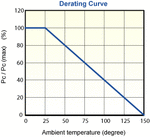
power derating.gif
This is the usual standard power de rating curve for silicon devices.

What it is saying is that the junction temperature must never exceed 150C.
The hotter the junction gets, the less additional power you can feed into it.

If your heat sink is already at 150C, then the rated power will be zero, because any extra power fed into the device would raise the junction temperature above the 150C maximum.

So the colder you can keep your heat sink, the more heat can flow out of the junction, and the more power you can feed into the device without the junction temperature exceeding 150C.

Devices are typically rated for a heat sink temperature of 25C which is just about impossible to achieve in practice, but it is the standard used.

A hypothetical device could have a rated power dissipation of 275 watts at 25C and de rated to 0 watts at 150C using the above curve.

A different way of rating the same device might be to say 275 watts de rated by 2.2 watts per degree Celsius of heat sink temperature rise.
.
If the temperature rise of the heat sink (above 25C) is 125C and you multiply that 125C rise by 2.2, you must de rate the device by 275 watts.

As its only a 275 watt device, de rating by 275 watts gets you to zero at 150C
 
Is that mean the less the derating factor the more the device can dissipate power and heat. for instance factor 0.5 W/c is better than 2.2 w/c
 

Is that mean the less the derating factor the more the device can dissipate power and heat. for instance factor 0.5 W/c is better than 2.2 w/c
No, a device that can flow 2.2 watts of heat per degree, can get rid of more heat than a device that can only flow 0.5 watts per degree temperature difference.

2.2W/C x 125C rise = 275 watt rated device at 25C
0.5W/C x 125C rise =62.5 watt rated device at 25C
 

The power is rated at a stated temperature. Read the fine print.

Above stated temp the manufacturer provides this derating
guidance.

A part with a SOA "corner-cut" starting at 125C (case) with
a 2C/W derating could be better for you (depending on real
case temp that you can hold, by your thermal design) than
a part rated at 70C with a -0.5C/W derating.

Details matter, they are where the marketing trickery hides.
 

The basic problem is that we cannot actually measure the junction temperature directly.

We need to use the manufacturers figures to calculate if the device is running safely below the maximum rated junction temperature, and the figures needed to do this can be presented in slightly different ways which can be confusing.
 

Status
Not open for further replies.

Similar threads

Part and Inventory Search

Welcome to EDABoard.com

Sponsor

Back
Top