Continue to Site

Welcome to EDAboard.com

Welcome to our site! EDAboard.com is an international Electronics Discussion Forum focused on EDA software, circuits, schematics, books, theory, papers, asic, pld, 8051, DSP, Network, RF, Analog Design, PCB, Service Manuals... and a whole lot more! To participate you need to register. Registration is free. Click here to register now.

[SOLVED] S-parameters from a RF Circuit

Status
Not open for further replies.

EduardoGS

Newbie level 5
Joined
Sep 22, 2016
Messages
9
Helped
0
Reputation
0
Reaction score
0
Trophy points
11
Location
Brazil
Activity points
127
S-parameters from a RF Circuit - Circulator created from LC resonators

Hello everyone.

I am trying to simulate, for my undergraduate thesis, a new RF circulator that was published by Nature Physics on article called "Magnetic-free non-reciprocity and isolation based on parametrically modulated coupled-resonator loops".

My doubt is how to create a setup that understands one RF signal (sweep from 140MHz to 200Mhz) modulated by a signal with fixed frequency (15Mhz) and that has phase 120º difference between each one. After this, my goal is to plot S parameters and see the transmission from port 1 to ports 2 and 3. My curent setup in Cadence Virtuoso use QPSS and QPSP. In ADS2011, my curent setup use HB Simulation. On both cases the results are not good.

I have the article and I can send to you to read and understand better the problem if you wish.

Best regards.
 
Last edited:

The question is reducible to "does HB support analysis of parametric amplifiers and similar circuits"? I fear it doesn't but I'm not working with ADS.

Analysis should be possible as transient analysis, extracting the questioned S parameters in post processing, although it's time consuming.
 

Modulation is only possible with nonlinear (active) devices, I presume.
My question was that, if the circuit is passive HB simulator will serve nothing.We shouldn't confuse nonlinearity of ferrite devices in standard circulator because this nonlinearity depends on the signal amplitude otherwise if this amplitude is relatively small, these components can be considered pseudo-linear.In order to check the transfer function of this circulator, I suppose a s-parameter simulation is enough.
 

I know that regular faraday effect circulators are linear passive devices. But the OP talks about modulation which isn't possible without non-linearity.
 

The circuit is not passive. The Larmor precession, that is a phenomenon that explains circulation through the ports in only one way, in this case occurs because the varactor diode. This device when receive the signal modulated with a different phase in relation to other (inserted another port) together with a RF signal, on the article, has the same results that a ferrite circulator, but without a magnet.
 

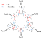
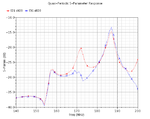
article_results.pngcircuit.png

All this figures were removed from article. On schematic figure, the ports 1, 2 and 3 are for RF and Modulation signals. Ports 4, 5 and 6 are for DC source, for to polarize a varactor diode. Note on the figure it contains a experimental setup made for them, that RF and Modulation signals are mixed using diplexers (The diplexers are for to block a RF signal in the other source, that produces a Modulation signal). Similarly, the schematic contains a specific device for make a shift of phase from Modulation Signal.

On another figure is possible to see the results. This circuit makes the same that ferrite circulator...
 
Last edited by a moderator:

The general characteristic of HB analysis suggests it can be used (from cktsim manual):
Harmonic Balance Overview
Harmonic balance is a frequency-domain analysis technique for simulating distortion in nonlinear circuits and systems. It is well-suited for simulating analog RF and microwave problems, since these are most naturally handled in the frequency domain. You can analyze power amplifiers, frequency multipliers, mixers, and modulators, under large-signal sinusoidal drive.

Harmonic balance simulation makes possible the multitone simulation of circuits that exhibit intermodulation frequency conversion. This includes frequency conversion between harmonics. Not only can the circuit itself produce harmonics, but each signal source (stimulus) can also produce harmonics or small-signal sidebands. The stimulus can consist of up to twelve nonharmonically related sources. The total number of frequencies in the system is limited only by such practical considerations as memory, swap space, and simulation speed.
 
I remember reading that article and being disappointed that it didn't describe how much power is needed for modulation, or what the effective linear range of the thing is. Based on that I'm betting that the working power level is much less than the power required to pump the varactors, so it would never be useful for high power applications...

I don't see why harmonic balance or PSS wouldn't be able to solve it. Are you having problem with convergence, or are the resulting waveforms just not looking correct?
 

    V

    Points: 2
    Helpful Answer Positive Rating
I have problems with the results. The waveforms shows a different of the article. I am making one simulation now. When it's over I'll put here.
 

ade_setup.pngresult1_with_vm.pngresult2_without_vm.pngschematic.pngschematic1.pngsetup_port.png

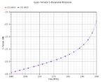
My results until this moment are these. The graphic where S21 is equal to S31 represents the simulation without Vm (modulation signal). Comparing the other graphic with the other posted on previous message, it contains the result from article, my results are wrong.

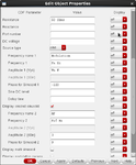
The others figures shows my schematic and testbench, includes ADE setup and Ports configuration. In the Port presented realizes it the "phase for sinusoid 1" is -120°. To others ports these parameters are 0° and +120°. The modulation's amplitude is 0.6V because is the same used on article.

Like "mtwieg" said, the RF power was not specified on article. I bet in 3dBm.
 

I think LSSP simulation may be feasible because it's not a ordinary circulator with ferrite core.LSSP will drive the circuit with a certain signal level but it's not possible to add a modulation to LSSP port.You may also do Envelope simulation in ADS ( if it's available) in order to see the spectrum at each port or You can do a PSS simulation by connecting a current measurement element then calculate input reflections and transfer functions of the ports by calculating voltages and currents in complex form.
 
Dear all,

Sorry about the article. I read the "right and permissions" from Nature Physics and I discovered that is illegal. Therefore, I removed from my dropbox.
The link for to buy the article and to see some important informations, like the results graphics: https://www.nature.com/nphys/journal/v10/n12/full/nphys3134.html

About the simulation, my goal is: see the power to flow from port 1 to 2 or port 2 to 3 or port 3 to 1, but not in the reverse direction. Beyond that the results need to show the non-reciprocity, e.g., S11 = -20dB, S31 = -20dB and S21 = 0 dB when the frequency is 170MHz (with BW = 10Mhz), the RF signal is inserted at port 1 and Vdc=1.99V.

The varactor (SMV1237 - the same used on article) was made following the spice model. ( Follow the link: https://www.skyworksinc.com/uploads/documents/Varactor_SPICE_Model_AN_200315C.pdf ). I made the simulations for to validate this model and my results are compatible with the one showed on spice model and with the description on article (C = 30pF when Vdc = 3V). The Diode_Model represents the diode used on varactor model designed. The "diode.scs" (represents Diode_Model) and "input_varactor.scs" (from varactor's testbench) were added on dropbox.

The figures on the folder contains the results of two situations. First one represents the case when no modulation signal was inserted. The article results shows that S21 are equal to S31 in that case described above. This means that without signal modulation this device behaves as power divider and not as a circulator. The second situation represents the case with the signal modulation and on this case, the device behaves as a circulator. The article reports that Vm = 0.6V (modulation signal voltage) and has no information about the RF signal. It also reports that Vdc = 1.99V (DC voltage inserted on ports 4 to 6 on the device). The Vdc is a frequency adjust. This means that if Vdc >= 1.73V and Vdc =< 4.50V the resonance zone is from 160Mhz to 210MHz. When Vdc=1.99 the device resonance zone is 170MHz.

On article besides the simulation it is contains the experimental setup. In this case, the signals RF and Modulation are generated by VNA (RF from 140MHz to 200Mhz) and Waveform generator (for 15MHz signal). The modulation signal is passes through a Power Divider and then by a Phase Shifter (because the three modulation signals need to have 120º on phase each other) and finally by a Diplexer. The low-pass ports of three diplexers receives the Modulation signals and the high-pass ports receives the VNA. Then the output of diplexer is connected at ports 1 to 3 of device.

Best regards,
Eduardo.
 

Status
Not open for further replies.

Part and Inventory Search

Welcome to EDABoard.com

Sponsor

Back
Top