Continue to Site

Welcome to EDAboard.com

Welcome to our site! EDAboard.com is an international Electronics Discussion Forum focused on EDA software, circuits, schematics, books, theory, papers, asic, pld, 8051, DSP, Network, RF, Analog Design, PCB, Service Manuals... and a whole lot more! To participate you need to register. Registration is free. Click here to register now.

[SOLVED] RF Signal spectrum content explanation

Status
Not open for further replies.

johnny_b4e

Newbie level 5
Joined
Nov 22, 2012
Messages
10
Helped
0
Reputation
0
Reaction score
0
Trophy points
1,281
Activity points
1,364
I have transmitter outputting a CW signal at 869.000200 MHz.
In spectrogram I see other symmetrical peaks spaced at 165kHz.
spectrum.png

Clock source is 26MHz TCXO. I was thinking what is the source of them.
 

Spurs from a switching power supply? You haven't given us enough info about your system to do anything more than guess.
 

About system:
Power supply is mains AC transformer adapter to 12V, then generic 3.3V regulator.
Transmitter is Si4468 as class E amplifier with bias voltage from LDO (TPS73201).
Output goes trough two RF switches SKY13323-378LF and SKY13385-460LF
TCXO is EPSON TG-5006CG

Also, a guesses would be totally fine. Maybe I find out something interesting or new that way.
I was thinking maybe that's from internal fractional PLL.
 

Step the output down in frequency and see what the spurs do. If they change their offset freq, then it is most likely a frac-N spur.
 
I changed frequency twice (860 and 868), but the offset stays the same both times.
Also checked with battery supply, still the same offset.
And finally changed data rate and deviation. I know it shouldn't matter in CW mode, but checked anyway. Result was the same.

Many small radio PLL transceivers have spurs like this.

So the fact that peaks stay at constant offset mean that its from phase detector inside PLL?
Assuming that, if I would change clock source to slightly different frequency, the spur offset would
change?
 

I changed frequency twice (860 and 868), but the offset stays the same both times.
Typically, the spur pattern changes when switching the carrier frequency, and it's less regular due to the fractional synthesizer design. So there might be a different reason. Changing the crystal frequency is a useful test to see if the spurious signal is somehow related to PLL operation.

Can you exclude interferences from the controlling system, e.g. a microcontroller?
 
What about to play a bit with the PLL loop filter and/or with the the charge pump current...Might be possible through the registry settings.
Tuning the PLL loop filter there will be a compromise between spur rejection, loop stability, and PLL frequency switching time.
 
I've done some testing.
I changed some settings of internal PLL CP and VCO, this reduced level of spurs.

But one interesting change was, when I switched microcontroller internal RC clock source
frequency. Changing clock resulted in changes in spur offsets.
Here I have to mention that this RF chip is embedded inside MCU (EZR32LG230).
Also my TCXO clock is buffered trough MCU and then fed to RF clock input. It was so I can
use it for both MCU and RF.

I assume that my RC clock was causing some spurs in addition to those naturally from PLL.
 

I've patched my clock source to go directly to RF clock input and that removed all visible
spurs and reduced noise levels a bit.

So in conclusion there was interference on clock signal due to bad design.
 

I've patched my clock source to go directly to RF clock input and that removed all visible
spurs and reduced noise levels a bit.

So in conclusion there was interference on clock signal due to bad design.
But your signal has still very bad spectral purity.Especially PN seems horrible.
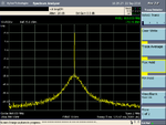
 

But your signal has still very bad spectral purity.Especially PN seems horrible.

Here is latest measurement with improved levels:
patched_clock.png
Note that span is 2MHz compared to initial!

Datasheet states PN= -105 dBc/Hz at 10kHz offset. So if 1kHz BW then should be -75dBc? And I have -50dBc.
I guess its quite bad if I calculated correclty.
 

Here is latest measurement with improved levels:
View attachment 132396
Note that span is 2MHz compared to initial!

Datasheet states PN= -105 dBc/Hz at 10kHz offset. So if 1kHz BW then should be -75dBc? And I have -50dBc.
I guess its quite bad if I calculated correclty.

The calculation is not done as you did with spectrum analyzers, you should add a correction factor coming from spectrum analyzer...
But anyhow the spectrum is still too bad.Either you make a measurement mistake or your circuit is really bad,I think you'd check out you circuit precisely.
 

Status
Not open for further replies.

Part and Inventory Search

Welcome to EDABoard.com

Sponsor

Back
Top