Continue to Site

Welcome to EDAboard.com

Welcome to our site! EDAboard.com is an international Electronics Discussion Forum focused on EDA software, circuits, schematics, books, theory, papers, asic, pld, 8051, DSP, Network, RF, Analog Design, PCB, Service Manuals... and a whole lot more! To participate you need to register. Registration is free. Click here to register now.

RF Trace Layout question

Status
Not open for further replies.

sschocke

Newbie level 4
Joined
Jun 26, 2016
Messages
5
Helped
0
Reputation
0
Reaction score
0
Trophy points
1
Location
Vanderbijlpark, South Africa
Activity points
59
I came across this thread on the forums regarding RF Trace design for a SIM900 module because I have designed a PCB using the same module, but I am having terrible trouble with it. I have come to the conclusion after much experimentation that I have made some grave mistake with the antenna part because the modem's communication on the GSM network causes such terrible interference that the microcontroller actually freezes up, unless I rotate the antenna connector on the PCB side a certain way... and even then, it's still not 100% stable.

After reviewing the original post, I can now see that a 0.254mm trace width for the antenna with very little ground clearance on the top ground plane would definitely cause major trouble. I have updated my design, but I need some input on whether I am just making another mistake, or whether the changes will actually make a difference.

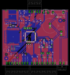
Please find attached below the layout in question.
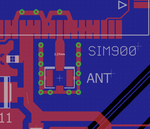
AntennaTraceV1.png

Any and all input is welcome. I am a novice when it comes to RF antenna traces. We have always used modules with embedded antenna connectors on previous projects.

Kind Regards,
Sebastian
 

I don't think that the antenna trace causes particular problems. Most serious problem is most likely having too few ground vias, also probably ground plane discontinuity. We need to see the full design.

Another question is if the said interferences are possibly observed with a GSM antenna near to the board. If so did you try to displace it to a distant position?

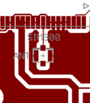
In regards to the antenna trace, I just want to make sure everyone understands the attached design is how I want to do it in future... below is the current layout that is giving me problems.
AntennaTraceOld.png
*Bottom ground plane not shown

As requested, here is the full design:
FullDesignV1.png

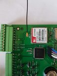
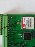
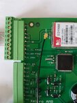
To understand why I have mentioned that it must be something related to the board design, specifically the antenna, I need to show some pictures:
photo_2016-06-27_06-54-58.jpg photo_2016-06-27_06-55-04.jpg photo_2016-06-27_06-55-08.jpg

In the first photo, everything works perfectly. In the others, the micro freezes up every time it transmits on the GSM network.

Regarding your last suggestion, I have moved the antenna far away by using a pigtail and an external antenna located a good 1.5m away from the board. This gave me both better signal and made the problem worse. With the external antenna I need to orient the connector to a certain rotation, and pull the pigtail straight up vertically away from the board to ensure the micro does not freeze up.

Also, it is not a power supply related problem. Have analyzed it extensively throughout using an oscilloscope.
 

According to the SIM900 Application Note, both neighbor pins 59 and 61 must be tied to ground, which is clearly suggested by seeing the inner connections you routed bellow IC footprint, however it is strange that copper plane around antenna connector do not reach these pins. Are you sure that this plane is really connected to the ground ?
 
Yes, I am quite sure they are connected, but the reason for them not being connected to the pins is that I manually drew the "ground plane" around the connector using the via's and tracks. I have specifically put down a "keepout" region around the connector so the ground plane would not automatically fill in there. I saw quite a few other boards online had the same concept where even if there was a top ground plane, they would not have it around the antenna trace, and I figured this may be part of my problem.

I can connect the two topmost via's to the ground pins on the IC like this easily enough, if that would make it better?
AntennaLayoutV2.PNG
 

YI saw quite a few other boards online had the same concept where even if there was a top ground plane, they would not have it around the antenna trace, and I figured this may be part of my problem.

I can connect the two topmost via's to the ground pins on the IC like this easily enough, if that would make it better?

I have to admit that I never used this chipset, but according the the layout guideline (5) on page 8 of the same document, it is strictly stated that the ground plane must be everywhere, and we can see an illustration of that at the following pictures at page 9, where the ground plane covers all the neighbor regions. The fact that other designs worked not following these directives it do not mean that the same should happens as well with your design.
 
Status
Not open for further replies.

Part and Inventory Search

Welcome to EDABoard.com

Sponsor

Back
Top