Continue to Site

Welcome to EDAboard.com

Welcome to our site! EDAboard.com is an international Electronics Discussion Forum focused on EDA software, circuits, schematics, books, theory, papers, asic, pld, 8051, DSP, Network, RF, Analog Design, PCB, Service Manuals... and a whole lot more! To participate you need to register. Registration is free. Click here to register now.

RF Trace design for GSM module

Status
Not open for further replies.

DrBudz

Junior Member level 3
Joined
Dec 5, 2011
Messages
28
Helped
0
Reputation
0
Reaction score
0
Trophy points
1,281
Activity points
1,500
Hi friends,

I need help to design trace from module's RF pin to the SMA connector. Impedance of the SMA connector is 50ohm.
I want to connect GSM module SIM900 to SMA connector, and then to connect GSM antenna to SMA connector.
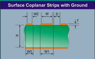
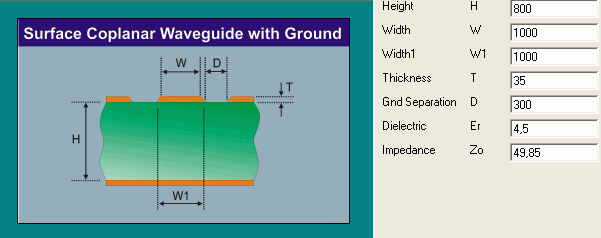
In SIM900 datasheet is written that the RF trace for the antenna pad should have 50ohm impedance.

Does that trace need to be 50ohm impedance if I use 50 ohm SMA connector?
How can I tune that trace to 50ohm impedance?
Is there any required distance between RF trace and ground plane?

It's a 2 layer board.
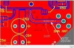
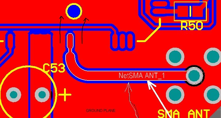
Here is the image of the RF trace from module to SMA connector
Top layer is red, bottom layer is blue.
sim900.jpg

Thank you!
Best regards!
 

Does that trace need to be 50ohm impedance if I use 50 ohm SMA connector?

If the line length is not << wavelength, you should try to design the line width with proper line impedance.

For double sided FR4 with 1.5mm distance between signal and ground, the line with for 50 ohm is ~2.7mm. That is really wide, and you will not be able to keep that width everywhere, but at least try to use the proper line with where you can.
 

Thanks Volker.

What about ground plane on top layer? Should I keep the distance between ground plane and RF trace like this:
distance=3*RF_width ?
 

What about ground plane on top layer? Should I keep the distance between ground plane and RF trace like this
Not necessarily. You can also design the line as coplanar strip, embedded between ground traces, allowing 50 ohm impedance with possibly less ocupied space. The ground traces should have multiple ground vias (a via "fence"). It depends on your technology parameters like minimal via size, if it makes sense.

According to my experience coplanar with ground is always an option to implement lower impedance traces with thick substrate PCBs.

39_1323286535.jpg
 
  • Like
Reactions: DrBudz

    DrBudz

    Points: 2
    Helpful Answer Positive Rating
What is the distance (D) between via fence and RF trace?
Can I use ground plane on top layer and than place vias to create via fence?
I'll check tomorow with the pcb manufacturer about minimal via size and pcb layer thicknes, and I'll post it here.
Thank you!
 

For a 1.6 mm double layer FR4 board, the required ground isolation is about 0.15 mm, which should be feasible.

P.S.: Based on the actual trace width of about 0.5 mm
 
Last edited:
  • Like
Reactions: DrBudz

    DrBudz

    Points: 2
    Helpful Answer Positive Rating
For a 1.6 mm double layer FR4 board, the required ground isolation is about 0.15 mm, which should be feasible.

You can do that, but that's an entirely different line type and the line width that I specified is no longer valid. The line will be (much) narrower if you have ground metal on the sides.

---------- Post added at 21:58 ---------- Previous post was at 21:55 ----------

What about ground plane on top layer? Should I keep the distance between ground plane and RF trace like this:
distance=3*RF_width ?

If you want ground on that layer, then this distance should be safe, i.e. the line is still close to microstrip and my calculated value is valid. If ground is much closer (and connected to the bottom ground with via fence), then the line width must be smaller.
 

You should preferably place individual ground vias for all ground pins of the SIM900 module. Then the coplanar ground can be easily connected at the module side.

Small industry standard vias like 0.6 mm pad 0.3 mm drill should be O.K.
 
  • Like
Reactions: DrBudz

    DrBudz

    Points: 2
    Helpful Answer Positive Rating
I've asked pcb manufacturer about via size and board thickness.
Minimum via size is 20mil drill and 45mil pad.

Board thickness options are 0.8mm, 1mm, 1.5mm, 2mm. Copper thickness is 18u and 35u.
 

45 mils via pads is huge for SMT technology in my view, but it should be sufficient to connect the SIM900 module with 1 mm pad spacing, at least when using a zigzag pattern. I would go for 0.8 mm substrate, you get about 1.4 mm (55 mils) trace width for 50 ohm microstrip. Besides smaller 50 traces, thinner substrate has a main advantage of lower via inductance.
 
  • Like
Reactions: DrBudz

    DrBudz

    Points: 2
    Helpful Answer Positive Rating
Thanks, I'll go for 0.8mm board. Width of the RF trace is now as you suggested, about 1.4mm. How to calculate the distance between RF trace and top GND plane?
Here is the image of the RF trace and GND Plane.Sim900.jpg
 

How to calculate the distance between RF trace and top GND plane?
Here is the image of the RF trace and GND Plane.View attachment 65427

What you picture shows is really bad for RF.

If you have top side metal near the signal line, make sure that it is connected to the bottom side ground at least on both ends, and also with some additional vias in between. See attached screenshot with x for additional vias. And make sure that the signal line width is properly calculated, to account for the extra capacitance between signal line and the coplanar grounds. I have not checked the dimensions that FvM has suggested.

(As a microwave engineer, I prefer regular microstrip lines which have only the signal line of the top layer, without that additional ground on the sides.)
 

Attachments

  • vias.JPG
    vias.JPG
    96.3 KB · Views: 263
The ground plane is connected at both sides now, vias aren't shown or missing. I guess about 1.3 mm width, which would be correct without coplanar ground traces. Reasonable coplanar waveguide with ground parameters are e.g. 1.0 mm trace width and 0.3 mm ground separation.

 
  • Like
Reactions: DrBudz

    DrBudz

    Points: 2
    Helpful Answer Positive Rating
The ground plane is connected at both sides now

With sides, I meant both ends of the transmission line. In the screenshot, the top side metal is not connected to the bottom side ground at the module package. Depending on where the module's RF ground is, ground return current can not flow through top or bottom side ground. Try to fix that by connecting the grounds.

From my experience, grounds on both sides which are not properly connected are a common issue for RF circuit failure. Designers think "here's my ground" but current can not flow because current would need to change level, and there's no via in that place. Now the current needs a long path to reach some via somewhere -> extra inductance.
 
Last edited:

With sides, I meant both ends of the transmission line.
Yes, obviously.

The SIM900 antenna pin is placed between ground pins at both sides, that must be connected anyway. Unfortunately, the solder mask isn't shown in the artwork, but I símply assumed, that there must be some vias around it.

In fact the direct, lower inductance path to connect the module RF output is the bottom side.
 
The SIM900 antenna pin is placed between ground pins at both sides, that must be connected anyway.

It is connected on the top side of the PCB, so there is a continuous ground path between module and the antenna on the top side.

But how can return current flow through the bottom side ground from the module to the antenna?
It would have to flow from the module ground pin on the top side to the next via --- but that path is broken. Typical mistake in doing RF layout.

27_1323452796.jpg
 

You are completely right, if the ground vias would be omitted. I made in clear in my previous post, that I expect individual ground vias for each module ground pin. The good point is, that all ground pins are connected by a continuous ground plane on the module, but that's no reason to omit vias at the PCB.
 
  • Like
Reactions: DrBudz

    V

    Points: 2
    Helpful Answer Positive Rating

    DrBudz

    Points: 2
    Helpful Answer Positive Rating
Thank you guys, you are great.
I've added vias to connect top gnd and bottom gnd. Here is the picture with TOP Solder displayed.
What do you think about it now? Is it better?sim900TopSolder.JPG
 

Surely better. I would place some more vias directly beneath the ground pads (green in the below drawing), and possibly reroute the trace behind the antenna terminal at a larger distance to allow for ground vias at the other side of ground pins, too. Did you notice my latest calculation of 50 ohm trace?

 
Thank you.
What do you think now?
I've changed now trace width to 1.0mm, added new vias as you suggested, and rerouted trace to larger distance.
Here is the picture.sim900TopSolder.JPG
 

Status
Not open for further replies.

Part and Inventory Search

Welcome to EDABoard.com

Sponsor

Back
Top