Continue to Site

Welcome to EDAboard.com

Welcome to our site! EDAboard.com is an international Electronics Discussion Forum focused on EDA software, circuits, schematics, books, theory, papers, asic, pld, 8051, DSP, Network, RF, Analog Design, PCB, Service Manuals... and a whole lot more! To participate you need to register. Registration is free. Click here to register now.

Eagle CAD design quesiton

Status
Not open for further replies.

alpha91

Full Member level 3
Joined
Sep 23, 2011
Messages
168
Helped
1
Reputation
2
Reaction score
2
Trophy points
1,298
Activity points
2,625
Hi all, i just started to learn Eagle CAD to design PCB.
May I ask is it the trace overlap with via means they are connected when the board is fabricated?
i ask this because i am design without schematic.
For example like picture below:
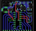
pcb.JPG

and i realize when i connect the trace to my parts, it pop out something like this (connect signal)
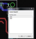
signal connection line.JPG

May i know what does it means?
 

Hi,

I assume you did not draw a schematic. Did you?
--> I recommend to first draw a schematic ... then generate the board from the schematic data.

It seems you are drawing lines as with a pencil.. but this is not the way one does with a CAD software.
EAGLE is intelligent and helps you to route the signals more efficentely.

I recommend to go through the tutorials. Step by step.

*****
To your problem:
You see that the errors says S$18 and S$19.
You can use "show S$18" to highlight the signal.
The same for S$19.

A connection from one pin of one device to another pin to another device usually is shown by a "signal", at first it is a airwire in the "unrouted" layer.
Select "route". then select an airwire and EAGLE generates a trace from it. It shows you the start point and the end point.
Select a 45° wire angle (or ther trace bend mode with the right mouse key) and place the trace. you may choose another layer (witout leaving the "route" command) and automatically EAGLE generates the via at the right place.
Usually you don´t place the vias by hand.

Klaus
 
You do not need those vias, for the red tracks come directly out of the pin, as a PTH component it will provide a better through connection.
 
Hi,

I assume you did not draw a schematic. Did you?
--> I recommend to first draw a schematic ... then generate the board from the schematic data.

It seems you are drawing lines as with a pencil.. but this is not the way one does with a CAD software.
EAGLE is intelligent and helps you to route the signals more efficentely.

I recommend to go through the tutorials. Step by step.

*****
To your problem:
You see that the errors says S$18 and S$19.
You can use "show S$18" to highlight the signal.
The same for S$19.

A connection from one pin of one device to another pin to another device usually is shown by a "signal", at first it is a airwire in the "unrouted" layer.
Select "route". then select an airwire and EAGLE generates a trace from it. It shows you the start point and the end point.
Select a 45° wire angle (or ther trace bend mode with the right mouse key) and place the trace. you may choose another layer (witout leaving the "route" command) and automatically EAGLE generates the via at the right place.
Usually you don´t place the vias by hand.

Klaus

Hi, yes, i am not using schematic.
i am using the pencil tools to draw it. do you mean it actually works but just that it is not the proper way to do it? or actually my board is not connected at all?
I will try to learn the schematic design.

You do not need those vias, for the red tracks come directly out of the pin, as a PTH component it will provide a better through connection.

i see. because i am doing manual connection (not convert from schematic)
will this affect?
 

I think the eagle asking you to that want you to connect the signals named S$18 and S$19.
attach the file to check the forum members that may more result
 
Hi,

Hi, yes, i am not using schematic.
i am using the pencil tools to draw it. do you mean it actually works but just that it is not the proper way to do it? or actually my board is not connected at all?
I will try to learn the schematic design.

EAGLE is flexible:
Even without schematic you coud use the "manual routing" features. (But I don´t recommend to work without schematic)
* ADD all the parts.
* use SIGNAL to tell EAGLE what pads should be connected.
* then use ROUTE ..it is almost the same as with a schematic.

Klaus
 
It's kind of silly (RE:stupid) to not first draw a schematic. A schematic is much easier to make the correct connections. On a board, not so much. Once you have made the correct connections in the schematic, it is difficult to not do the routing correctly on a board.

Do yourself a favor and create your schematic in the Eagle schematic editor. Then your board will be a breeze to complete.
 
I think the eagle asking you to that want you to connect the signals named S$18 and S$19.
attach the file to check the forum members that may more result

View attachment 16f628a.rar

My board file is attached. thanks.

Hi,


EAGLE is flexible:
Even without schematic you coud use the "manual routing" features. (But I don´t recommend to work without schematic)
* ADD all the parts.
* use SIGNAL to tell EAGLE what pads should be connected.
* then use ROUTE ..it is almost the same as with a schematic.

Klaus

Ok. thanks for your advice. I previously is using this method but i realize i cannot connect to via.
i will try for my next design.
but with my current design, does it actually connected?

It's kind of silly (RE:stupid) to not first draw a schematic. A schematic is much easier to make the correct connections. On a board, not so much. Once you have made the correct connections in the schematic, it is difficult to not do the routing correctly on a board.

Do yourself a favor and create your schematic in the Eagle schematic editor. Then your board will be a breeze to complete.

ok. thanks for your advice.
 

I think you should go to the "Help" button in the menu of the software or search for FAQ's then you can solve it.
 
Status
Not open for further replies.

Part and Inventory Search

Welcome to EDABoard.com

Sponsor

Back
Top