Continue to Site

Welcome to EDAboard.com

Welcome to our site! EDAboard.com is an international Electronics Discussion Forum focused on EDA software, circuits, schematics, books, theory, papers, asic, pld, 8051, DSP, Network, RF, Analog Design, PCB, Service Manuals... and a whole lot more! To participate you need to register. Registration is free. Click here to register now.

[SOLVED] RF Transmission Line(CPWG)

Status
Not open for further replies.

khankim

Newbie level 3
Joined
Mar 13, 2009
Messages
3
Helped
0
Reputation
0
Reaction score
0
Trophy points
1,281
Location
Seoul, Korea, South Korea
Activity points
1,301
Hello guys.

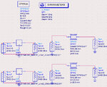
I designed 2.59-GHz RF PCB Module using FR-4 substrate.
For RF connection, I'm using CPWG(Coplanar Waveguide w/ GND) on the PCB.
Test RF pattern, attached fig1, is drawn to know how it produces rf loss at the desired frequency.
And the pattern is measured using by network analyzer Agilent 8753.
The results was totally different as my expectation, so I compare s-parameter between the ideal CPWG line and test pattern.
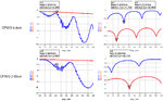
Attached fig2, fig3 are ADS schematic and simulation&measurement results.
Blue line is the measurement, red line is the simulation.
As you can see, the measurement results has large variation, especially S21 along the frequency.
Is there someone who know why such that big difference between simulation and measurement occur?

Thanks in advance
KhanKim
 

Attachments

  • fig1.jpg
    fig1.jpg
    85.6 KB · Views: 109
  • fig2.jpg
    fig2.jpg
    258.8 KB · Views: 110
  • fig3.jpg
    fig3.jpg
    286.4 KB · Views: 105

The transmission line dimensions appear to be fine, so your problem is likely a result of the mismatch at the connectors due to the narrow gap between the ground flood and the large center conductor of the (SMA?) connectors. If the center conductor is a thru-hole type, the same concern may be present on the backside GND flood as well. In addition, there is a small mismatch generated from the center-conductor passing through the board, serving as a stub. I assume that your simulation was just on the schematic portion which assumes ideal termination layout, and not an EM level simulation that factors in your actual layout characteristics. If you address the terminations, your measurements will be closer to the simulation. If you can do an EM simulation on the layout, that would be great too, but that is an extra cost for the ADS package.

You can try trimming away the ground plane near the center conductors to see if that helps resolve your problem. It also is beneficial to review the S11 & S22 measurements on the smith-chart format as opposed to a log-mag plot when measuring on the VNA... you will have a better grasp on what the impedance is. You can play around with some passive caps and inductors near the connectors to try to tune out your mismatch and optimize your loss for your 2.59GHz target band.
 
gap on end pads of transmission line appears too small resulting in null at 0.5GHz ? ( not shown) which shifts harmonic nulls down and shows 2GHz recursive S11 nulls.
 
I really appreciate your helpful reply.
I should study about the sma connector at the high frequency.
Thanks 'toohec'

KhanKim

- - - Updated - - -

I appreciate your helpful reply.
I should study about the thru-hole type sma connector.
Thanks 'toohec'

KhanKim
 

Be warned the CPWG component in ADS was broken. At least it was in ADS 2008 and all previous versions. I discussed it with Agilent tech support at the time and they confirmed it was bad. If you want to confirm if its still broken in your version or if they fixed it, do this simple experiment. Compare a Microstrip line (MLINE) to a CPWG with the gap set to a very high value and all other parameters the same. In this scenario the two results should be identical. If they are not at least close its still broken.

I don't know if this is your problem, but wanted you to be aware of it.
 

Status
Not open for further replies.

Part and Inventory Search

Welcome to EDABoard.com

Sponsor

Back
Top