rocky79
Member level 5
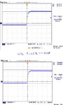
I have a switching regulator that operates at switching frequency of 260Khz that steps down a 28vdc to 3.3Vdc. The switching regulator output will supply current as high as 1 amp for the initial 5 minutes on power up then it falls off to several mAs.
Can you please suggest an input and output filter that dramatically reduces the input and output ripple as well as the high frequency noise?
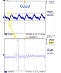
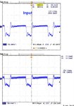
HF noise is measured to be in the 200~300Mhz range. I have attached the schecmatics as well as the input and output waveform as captured by the scope
Can you please suggest an input and output filter that dramatically reduces the input and output ripple as well as the high frequency noise?
HF noise is measured to be in the 200~300Mhz range. I have attached the schecmatics as well as the input and output waveform as captured by the scope
")