Continue to Site

Welcome to EDAboard.com

Welcome to our site! EDAboard.com is an international Electronics Discussion Forum focused on EDA software, circuits, schematics, books, theory, papers, asic, pld, 8051, DSP, Network, RF, Analog Design, PCB, Service Manuals... and a whole lot more! To participate you need to register. Registration is free. Click here to register now.

Help me understand a paragraph from a book (002)

Status
Not open for further replies.

samy555

Full Member level 4
Joined
May 11, 2010
Messages
207
Helped
0
Reputation
0
Reaction score
0
Trophy points
1,296
Location
Palestine
Activity points
2,963
Hello
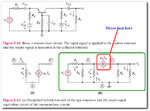
From " Semiconductor Devices and Basic Applications " page 435, the book talks about:
10.jpg
2.jpg
Figure 6.63 (b) is the small signal equivalent circuit. Notice that the dependant current source directed from the collector to the emitter.
In other pdf file I found in:
**broken link removed**
On page 137 the followinf small signal equivalent circuit:
3.jpg
Here the dependant current source directed from the Base to the Collector.
My question: Is these MODELS are equivalent? If yes, how?
Thank you
 
Last edited:

The main point that I need answered is how the dependent source in one is connected between C & E and in the other is between B & C???
 

Yes, it would seem the the dependent source should be between C & E in the second equivalent circuit also.
 

Yes, it would seem the the dependent source should be between C & E in the second equivalent circuit also.
Many of the books put the dependent source between C & B rather than C & E, please take a look at the attachment file, the dependent source is between C & B.

- - - Updated - - -

Also look the doc attached file
 

Attachments

  • t_model__hybrid_pi_model.pdf
    4.3 MB · Views: 111
  • The Common Base Amplifier.doc
    121.5 KB · Views: 84

I have started some rough literature researches - and the result is: Yes - we can find two different approaches for building a small-signal equivalent diagram for the common base (CB) case.
It is common to represent the BJT alone using a current source (gm*Vbe) between collector and emitter.
This applies also to transistor amplifiers in CE and CC configuration.
However, it is true that for CB configurations we have two choices:

1.) For the current source itself it makes no difference if it is connected to the (grounded) base or to the emitter because the input voltage source (at the emitter) provides a short to ground.
2.) If the controlled current source is between C and E it is NOT possible to divide the input and the ouput part of the circuit into two separate parts. As a consequence, the equivalent circuit diagram contains an input resistance that is identical to the CE and CC configuration (called hie or h11 or r(pi) ). In this case the current source Gm*Vbe must be considered during input resistance calculation (and causes the total input resistance to be rather small: 1/gm).
3.) Similar to the CE and CC case it is desirable to have no current path between the input and the output part of the circuit. Therefore, the current source in this version of an eqivalent small-signal diagram contains a a current source between C and ground (base). However, in this case, the left-sided input resistance must have the final value of 1/gm.

4.) Summary: Two versions are possible (current source between C-E or C-B), but the modelling of the input resistance also is different in both cases.

EDIT: As an example, in the second referenced document (*.doc) consider the second form of the equivalent small-signal diagram. Both parts are not connected via a current path. But you can lift the ground connection of the current source and connect it to the node E. The current still goes (through the signal source) to ground, but the value of the input resistor must be chaged at the same time from a low value (1/gm) to some kOhms (hie=h11=hfe/gm=h21/gm)
 
Last edited:
  • Like
Reactions: samy555

    samy555

    Points: 2
    Helpful Answer Positive Rating
Thank you LvW for that very clear answer
The last point I would like to discuss around is related to the polarity of Vbe and the direction of the controlled current source.
In Fig. A, the controlled current source is directed from C to B and the polarity of Vbe is as shown
A.jpg
In Fig. B, there is the opposite
B.jpg
What is your comment about that?
Thanks
==================
Edit: Personally, I think "Fig. A" is the original, and that if I want the opposite direction of the controlled current source, it is necessary that to reverse the polarity of (Vbe) voltage.
 
Last edited:

Status
Not open for further replies.

Similar threads

Part and Inventory Search

Welcome to EDABoard.com

Sponsor

Back
Top