Welcome to our site! EDAboard.com is an international Electronics Discussion Forum focused on EDA software, circuits, schematics, books, theory, papers, asic, pld, 8051, DSP, Network, RF, Analog Design, PCB, Service Manuals... and a whole lot more! To participate you need to register. Registration is free. Click here to register now.
Start with the timing capacitor with no charge so its voltage is low then the output at pin 3 is high which turns on the transistor and light.
The 220k resistor slowly charges the timing capacitor until its voltage reaches the threshold of 4V then the output goes low and the transistor and light turn off.
With the output low then the 220k resistor slowly discharges the timing capacitor until its voltage reaches the threshold of 2V then the output goes high and the transistor and light turn on again.
The circuit repeats the above.
I do not know why the circuit has the pushbutton and two 10k resistors voltage divider.
This circuit toggles the output every time that the switch is pushed.
when the switch is off then node2,6=3v it means that output holds its previous state.
The out put can be '1' or '0'. Let's consider the first case which means:
node3=6v then leftsideofswitch=6v,
as the switch is pushed node2,6=6v for a short moment then the output is '0'.
But after releasing the switch, the previous state ('0') is hold.
The same procedures happen when the transaction is from '0' to '1'.
I assumed that you are familiar with 555!
I have never seen a 555 used in that alternate action circuit. The 555 draws a fairly high supply current even when it is doing nothing.
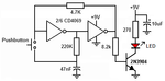
Here is another simple alternate action circuit that uses a cheap Cmos logic inverters IC that draws no supply current when it is doing nothing:
Can you please explain why we are using such values (220K resistor and 220nF capacitor) ? What's their effect in the circuit. Can I use some other values ?
- - - Updated - - -
@Audioguru
Wow, your circuit is just AWESOME !! Can you please explain how it works ? I've tried searching in google... But haven't found this schematic.
The product of RC(=220n*220K=48.4ms) introduces a time constat, by which "leftsideofswitch" approaches toward node3.
It means that "leftsideofswitch" would not reach node3 immediately.
I think that this RC path acts as a debouncer. You can search for the concept of "contact bounce".
So, when the switch is pushed, it takes 48.4ms for "leftsideofswitch" to reach 0v or 6v. Consequently, it takes a ratio of 48.4ms to reach 2v and 4v which are critical voltages for 555 to change its state. Using this, one could be sure that the output would not fluctuate during the "short moment" when the operator holds the pushbutton.
If RC is too much, then it will not let you to toggle one state after the other after a short period. If RC is too small, then the task of debouncing will not be accomplished.
So you can use other values near these R and C, however, appropriate values are determined depending on type of pushbutton and frequency of switching.
This site uses cookies to help personalise content, tailor your experience and to keep you logged in if you register.
By continuing to use this site, you are consenting to our use of cookies.