Continue to Site

Welcome to EDAboard.com

Welcome to our site! EDAboard.com is an international Electronics Discussion Forum focused on EDA software, circuits, schematics, books, theory, papers, asic, pld, 8051, DSP, Network, RF, Analog Design, PCB, Service Manuals... and a whole lot more! To participate you need to register. Registration is free. Click here to register now.

Removing settling time of a signal

Status
Not open for further replies.

patan.gova

Full Member level 3
Joined
Dec 19, 2011
Messages
172
Helped
4
Reputation
8
Reaction score
0
Trophy points
1,296
Activity points
2,776
Hello,
I am working with the pulse signals.My circuit is working fine but the output of the photodiode (pulse signal) is taking some settling time(shown with RedBox settling_time.JPGin the attached image) to come a an standard voltage level.
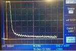
The output of the photodiode will be taken by switching it ON and OFF for some particular interval.I want to remove this settling time because when I want to take the output signal after 10sec of switching it ON then I don't get desired pulse signal as this will be still in settling stage.
Can anyone suggest how to remove the settling time.
Thanks.
 

Since your desired outcome is digital, move the threshold up
into the faster fall-time region. Then everything below / after
will be ignored.
 

@godfreyl :The horizontal scale is 2.5sec(it is shown at the bottom of the image).
@dick_freebird:I willl be just sampling the pulse signal form the analog board using microcontroller and later in matlab I will be performing the postprocessing of the signal.In the analog board I have two stages of filtering+amplification and the effect of settling time on the both stages are shown in the below image with the marked red region as settling time as I guess because after switching ON the supply for the LED the photodiode is taking around 4to5 secs of time to produce a pulse signal where the yellow signal represens first stage output and blue the second stage output.
Settlin_time_twostages.JPG
 

I presume the circuit behaves as designed. We need to review the circuit to understand why.
 

A bit of perspective:

The OP has about a dozen other threads about a heartbeat monitor circuit. If this is part of the same story, then he's completely screwed up the filter design, especially the second stage.

His original filter used an opamp running off a single-ended supply with no biasing, so it filtered, amplified, and then half-wave rectified the signal.

The only thing he seemed unhappy about was the small amount of ripple in the output, when the output was low. (This is also visible in the pictures above of the first stage output)

So he wanted to add a second stage of filtering to get rid of that ripple because it "didn't look nice". Instead, he seems to have invented a circuit that boosts the ripple out of all proportion, rather than eliminating it.

--------------------------------

My best advice would be to throw away the second stage, use the first stage as is, and connect it's output to a comparator with the threshold set to 1/2 the supply voltage - pretty much what Dick Freebird suggested in post 3 of this thread.

It's not as if the OP cares about the waveform or he wouldn't be half-wave rectifying it and clipping it in the first place.
 

@ godfreyl :Yes,you are right the output image shown above is from the circuit designed as same in this https://embedded-lab.com/blog/?p=5508.

The reason for using second stage is that the output pulse signal from the first stage is only of 200mV and the second stage making it as around 2V but I was aware of that the second stage will boosts the ripple out of all proportion, rather than eliminating it.Is it really doing.Can I get some more explanation on this.

Also how the 200mV pulse signal will look like if a comparator with a threshold set to 1.5 as the supply voltage is 3V and how much time the comparator will take to give out the otuput signal because the I need a fast processing analog circuit.
Thanks.
 

Both the scope traces you posted in this thread say "500mV", so I assumed the vertical scale is 500mV/division. If that's true, then the pulses inside the red boxes are about 3V in amplitude.

Also, the pulses in those pictures all have flat tops, indicating they have been clipped. IIRC, you are using a 3V supply, in which case we can expect that the pulses will be clipped at about 3V amplitude.

In any event, the 2'nd picture above says "CH1 500mV CH2 500mV", so presumably the scale is the same for the yellow and blue traces. Since the yellow and blue pulses inside the red box are both the same height, that means they are the same amplitude.

The reason for using second stage is that the output pulse signal from the first stage is only of 200mV and the second stage making it as around 2V
Huh? Your scope traces seem to show that the output pulses from the first and second stages are both 3V.

boosts the ripple out of all proportion, rather than eliminating it.Is it really doing.Can I get some more explanation on this.
On the yellow trace, the ripple outside the red box is much smaller than the pulse inside the red box. This is good.

On the blue trace, the ripple outside the red box is almost the same amplitude as the pulse inside the red box. This is bad.

Thus the second stage made the signal worse, not better.
 

I forgot to add one thing over here:when the power supply made ON then the both stages outputs are at 3V(inside the red box) and after this the first stage takes a lesser time to show up the dtetected pulse signal while the second takes takes a longer time to show up the detected pulse signals as in the image here
Sttling_time.JPG
 

To elaborate about previously stated "behaves as designed", it's quite normal that AC coupled circuits, particularly with single supply, need some time to settle to the final bias point, the lower the cut-off frequency and the higher the gain the longer the settling time.

In most cases, the settling tme would be just accepted, in special cases, e.g. battery operated circuit that are only mementarily powered, the settling time can be reduced by special design means.
 
Hello,
Now,I am planning to improve the working circuit design by minimizing the settling time.I really want to minimize this settling time.
@FvM :Can you explain me what kind of special design is needed to minimize the settling time.
Thanks.
 

Minimize your output capacitance (including the self-capacitance
of the driver) and minimize your load impedance. t=RC, R and C
is all you've got to work with. Presuming that the internal edges
are crisp, and not contributing to the fall time issue (not to be
assumed, base or gate shunt too weak can multiply the output
capacitance and produce a linear ramp, but this looks like a plain
RC characteristic, so...).
 

WIthout seeing the circuit, the problem with this design is that the photodiode appears to saturate with 3V across the current sense resistor and then the recovery time is extended, also as the current drops the RC time constant increases

The second problem is that the filter BW should match the signal content for optimum SNR to reject ripple. Some research is needed to determine this base on rise/tail time of expected pulse.

The third problem is there will be gain variation so unless the comparator a.k.a. PW50 slicer is variable, the pulse will shrink and stretch and more prone to noise.

Thus AGC is mandatory to allow for variation in emitter variation an path loss. THe AGC response time constant must be fast attack and slow decay.
 

Hello,
Can someone suggest me the modificatiosn needed in the circuit to minimize or remove settling time.
Thanks.
 

Settling time can often be an issue with photodiode circuits - especially when one is interested in such very low frequency signals and needs as much gain as your heartbeat monitor circuit. If you must use the particular photodiode you have, your choices might be more limited - but some photodiodes are designed to oeprate with moderate to high reverse bias voltages, which correspondingly reduces the device capacitance and speeds up the response & settling time. Some other options can be to use a servo amp to monitor and feedback offset voltage into your filter circuit when you are not in the measuring mode.
If you can access this web link, it may give you some useful information-
https://users.ox.ac.uk/~atdgroup/technicalnotes/Getting%20the%20best%20out%20of%20photodiode%20detectors.pdf
 

The circuit is being discussed at edaboard since more than 9 months, in seemingly innumerable threads. https://www.edaboard.com/threads/300281/#post1284822

Tpetar who suggested it stated "it works like a charm" but there have been also various comments about it's weaknesses.

Apparently the circuit startup time is your only concern. It's caused by the required charging of coupling (highpass) capacitors and is in so far "natural" behaviour of this particular circuit.

I believe that the startup time can be reduced by connecting clamping diodes across the 47k resistors, either standard Si or schottky.
 

Hello FvM thanks for your suggestion.I tired using IN4004 diodes across both the 47K resistors but the startup time is still the same(the usage of diodes not removing the startup time).
Can I get anymore suggestions regarding this startup time.
thanks.
 

Status
Not open for further replies.

Similar threads

Part and Inventory Search

Welcome to EDABoard.com

Sponsor

Back
Top