faisal78
Member level 3
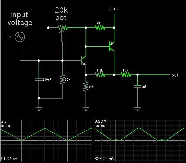
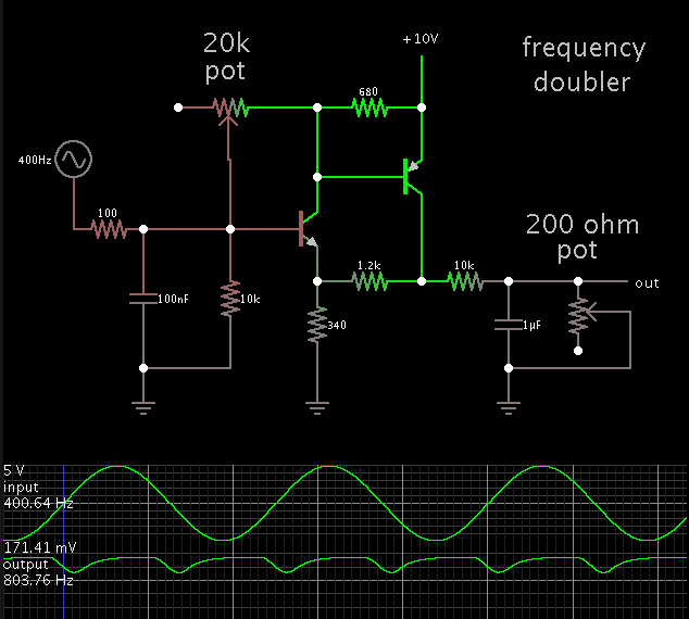
Hi
I was trying to figure out this circuit but could not figure out its operation.
I had done a simple simulation, it seemed to work as per intention, i.e. a DC voltage doubler/multiplier?..
Can somebody help me understand how it works and its circuit tradeoffs.
BTW - this is not the typical flying capacitor/switching diodes circuit. its only based on 2 BJT transistors.
Below are the schematic and the simulation results.
Essentially, the input (V1) is a voltage source from a DAC that can output from 0v - 4v.
The simulation results DC sweep on the x-axis is sweeping V1.
Output is monitored from C2 output cap.
As you can see from the results, once V1 exceed ~600mV which turns on Q1, the output starts to "double/triple" based on the input until saturation.