sarslanali
Junior Member level 2
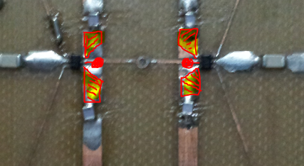
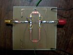
I am designing a phase array antenna for my final year project. For phase shifting part I am using skyworks SPDT Switch AS213-92LF. As there is no model available for simulating the switch, so I directly designed and tested the phase shifter. The PCB is shown in the picture. It is not final PCB, as you can see. The problem is that I am getting S11 about -6 db, S22 about -7 and S12 about -10 db, which is very poor performance. Please tell me what can I do to improve performance. I am using 50 ohm line on FR-4 substrate and operating frequency is 2.4 GHz. Please its urgent.