Georgy.Moshkin
Full Member level 5
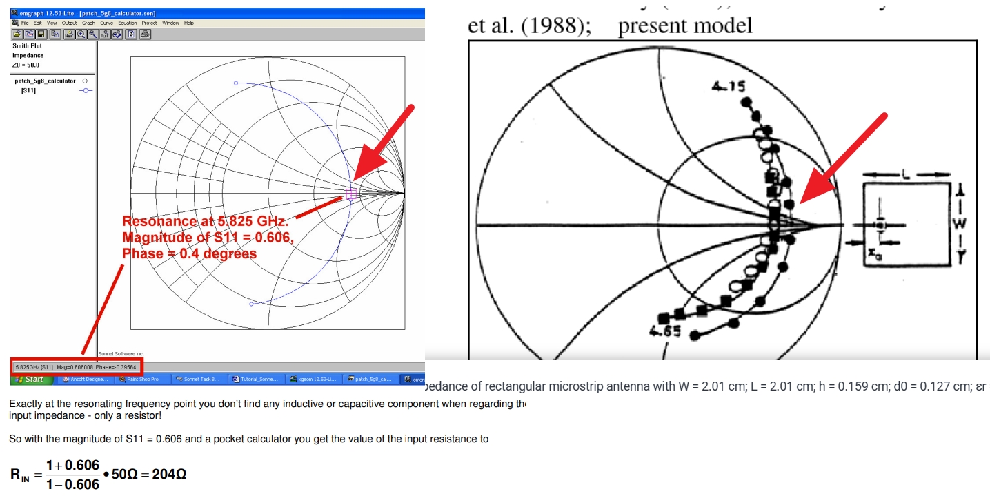
In many sources, e.g.,
patch input impedance point is placed on a real axis of Smith Chart:

This means that patch impedance is purely resistive and can be replaced with equivalent resistance (or conductance). This is very convenient when designing resonant series patch arrays, because we can use simple arithmetic. If we need to design 3-element series patch array with a 50 Ohm feeding line, we can tune single patch impedance to 3*50=150 Ohm and then connect three 150 Ohm patches in series.
So, the simulation assisted design steps are:
1. Connect 50 Ohm lumped port to the patch
2. Tune patch width/height till S-parameter curve crosses real axis at R=150 Ohm point
3. Create 3-patch array model
4. Simulate and tune patch width/height to compensate mutual coupling effects.
From my experience, it almost never works this way! The problem is that single patch S11 from simulation is often not purely real. S11 can be anywhere, e.g. at the bottom of Smith Chart, or somewhere in-between. This means that if we blindly use intersection of S11 curve and real axis, we will often get incorrect results. Thus, I am struggling to provide best practical steps to find single patch impedance that can be used to design resonant series array. Of course, it is possible to perform simulation for patch attached to a lumped port with required impedance R. E.g., if we use 150 Ohm port and tune patch width/height till its matched (point in the center of 150 Ohm Smith Chart). But after we connect these patches one by one in series connected by a 50 Ohm feeding line, we again end up with points that are not purely resistive, and array is far from being well matched, i.e. adding antenna elements is not directing antenna impedance to the center of Smith Chart. I thought that it happens due to mutual coupling effects between patch and feeding line, but if we compare S11 when feeding port is directly attached to the patch and when it is attached through half-wavelength line (impedance repeater), differences are more or less negligible. Thus, this S11 phase variations for different dimensions/substrates are caused by something else.
Few years ago, I came up with a simple approach to solve this problem. My approach is based on two ideas:
1) Perform three simulations: for 1-element, 2-element and 3-element arrays. Draw three S11 points at required resonant frequency. We can tune phase delay line and patch dimensions until we can draw a straight line through these points which is directed to the center of Smith Chart. This aligns well with resonant array equivalent circuit, where we add patches like a simple resistors and everything is linear and predictable.
2) Perform two simulations with first element feeding line L and L+90 degrees (increased by quarter wavelength). This helps to find a "hidden" impedance mismatch, because adding additional quarter wavelength portion will transform impedance somewhere else if it is not well matched.
While this approach works great for me, now I need to explain this to my students and keep it simple. I must admit that I don't clearly understand why this happens. My practical antenna design and manufacturing knowledge is much stronger than theoretical background. I observe that this effect varies for different substrate thicknesses, dielectric constants and patch dimensions. My current understanding that generally patch with a purely resistive resonance should have some small piece of feeding line attached, and this line L adds to patch RLC resonance model, so it becomes purely resistive on a Smith Chart. I would be glad if someone can explain why single patch S11 phase varies greatly for different substrates/dimensions. And what is your approach to design of series resonant arrays. Not by simply creating large models and brute-force optimize them.
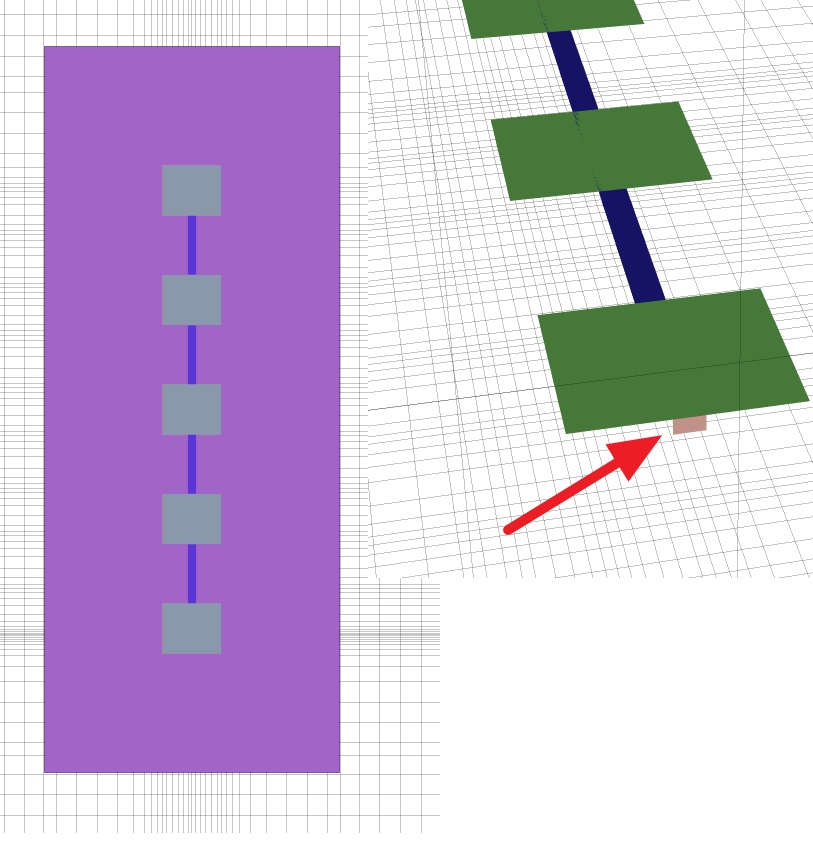
Edit: Here is how it looks like in OpenEMS and after simulation


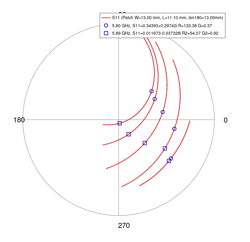
This chart shows 5 antenna arrays simulated in OpenEMS.
Circle - 5.8 GHz
Square - dip in S11
Center of Smith Chart - 50 Ohm
1-element array: Optimized dimensions, so square and circle have same resonant frequency 5.8GHz
2-, 3-, 4- and 5-element arrays: All patch elements have equivalent resistance of 250 Ohm. Equivalent circuit of resonant series array is N resistors connected in parallel. For two-element array R=250 Ohm / 2 = 125 Ohm
For three-element array R=250 Ohm / 3 = 83 Ohm
For two-element array R=250 Ohm / 4 = 62.5 Ohm
For two-element array R=250 Ohm / 5 = 50 Ohm
This case shows "correct" behavior. But in some cases, we will end up in wrong point on a Smith Chart. But if I use approach described above (tuning 1- 2- and 3- element array dimensions until their impedance points lay on a single line with center of the Smith Chart) then results are always correct.
patch input impedance point is placed on a real axis of Smith Chart:
This means that patch impedance is purely resistive and can be replaced with equivalent resistance (or conductance). This is very convenient when designing resonant series patch arrays, because we can use simple arithmetic. If we need to design 3-element series patch array with a 50 Ohm feeding line, we can tune single patch impedance to 3*50=150 Ohm and then connect three 150 Ohm patches in series.
So, the simulation assisted design steps are:
1. Connect 50 Ohm lumped port to the patch
2. Tune patch width/height till S-parameter curve crosses real axis at R=150 Ohm point
3. Create 3-patch array model
4. Simulate and tune patch width/height to compensate mutual coupling effects.
From my experience, it almost never works this way! The problem is that single patch S11 from simulation is often not purely real. S11 can be anywhere, e.g. at the bottom of Smith Chart, or somewhere in-between. This means that if we blindly use intersection of S11 curve and real axis, we will often get incorrect results. Thus, I am struggling to provide best practical steps to find single patch impedance that can be used to design resonant series array. Of course, it is possible to perform simulation for patch attached to a lumped port with required impedance R. E.g., if we use 150 Ohm port and tune patch width/height till its matched (point in the center of 150 Ohm Smith Chart). But after we connect these patches one by one in series connected by a 50 Ohm feeding line, we again end up with points that are not purely resistive, and array is far from being well matched, i.e. adding antenna elements is not directing antenna impedance to the center of Smith Chart. I thought that it happens due to mutual coupling effects between patch and feeding line, but if we compare S11 when feeding port is directly attached to the patch and when it is attached through half-wavelength line (impedance repeater), differences are more or less negligible. Thus, this S11 phase variations for different dimensions/substrates are caused by something else.
Few years ago, I came up with a simple approach to solve this problem. My approach is based on two ideas:
1) Perform three simulations: for 1-element, 2-element and 3-element arrays. Draw three S11 points at required resonant frequency. We can tune phase delay line and patch dimensions until we can draw a straight line through these points which is directed to the center of Smith Chart. This aligns well with resonant array equivalent circuit, where we add patches like a simple resistors and everything is linear and predictable.
2) Perform two simulations with first element feeding line L and L+90 degrees (increased by quarter wavelength). This helps to find a "hidden" impedance mismatch, because adding additional quarter wavelength portion will transform impedance somewhere else if it is not well matched.
While this approach works great for me, now I need to explain this to my students and keep it simple. I must admit that I don't clearly understand why this happens. My practical antenna design and manufacturing knowledge is much stronger than theoretical background. I observe that this effect varies for different substrate thicknesses, dielectric constants and patch dimensions. My current understanding that generally patch with a purely resistive resonance should have some small piece of feeding line attached, and this line L adds to patch RLC resonance model, so it becomes purely resistive on a Smith Chart. I would be glad if someone can explain why single patch S11 phase varies greatly for different substrates/dimensions. And what is your approach to design of series resonant arrays. Not by simply creating large models and brute-force optimize them.
Edit: Here is how it looks like in OpenEMS and after simulation
This chart shows 5 antenna arrays simulated in OpenEMS.
Circle - 5.8 GHz
Square - dip in S11
Center of Smith Chart - 50 Ohm
1-element array: Optimized dimensions, so square and circle have same resonant frequency 5.8GHz
2-, 3-, 4- and 5-element arrays: All patch elements have equivalent resistance of 250 Ohm. Equivalent circuit of resonant series array is N resistors connected in parallel. For two-element array R=250 Ohm / 2 = 125 Ohm
For three-element array R=250 Ohm / 3 = 83 Ohm
For two-element array R=250 Ohm / 4 = 62.5 Ohm
For two-element array R=250 Ohm / 5 = 50 Ohm
This case shows "correct" behavior. But in some cases, we will end up in wrong point on a Smith Chart. But if I use approach described above (tuning 1- 2- and 3- element array dimensions until their impedance points lay on a single line with center of the Smith Chart) then results are always correct.
Last edited: