therash09
Newbie level 2
- Joined
- Jun 14, 2011
- Messages
- 2
- Helped
- 0
- Reputation
- 0
- Reaction score
- 0
- Trophy points
- 1,281
- Location
- New Delhi, India
- Activity points
- 1,329
I am having problems in solving two questions belonging to Circuits.
Question 1 can be found at the link given below:
https://picasaweb.google.com/11636060715…
or
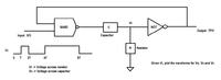
Given is a circuit having a pulsed aperiodic wave pattern, Vi. To be plotted are output waveform Vo, waveform across capacitor Vc and waveform across resistor Vr.
Question 2 can be found at the link given below:
https://picasaweb.google.com/11636060715…
or
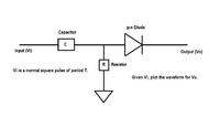
To be found is the output waveform Vo, if the input to the circuit is a uniform square pulsed wave pattern.
While I have been able to almost entirely do Question 2, there seems some very basic conceptual error not leading to the correct answer. As for Question 1, I could find very little headway.
It would certainly not be possible for anyone to plot the waveforms here, and I do not expect anyone to plot the same for me on any other platform. What I require is the method to proceed with these questions and the steps, particularly for Question 1. The required waveforms could be vaguely mentioned in statements, as these answers shall be of utmost help, alongside the methodologies!
I will be extremely thankful to everyone who answers!
Question 1 can be found at the link given below:
https://picasaweb.google.com/11636060715…
or
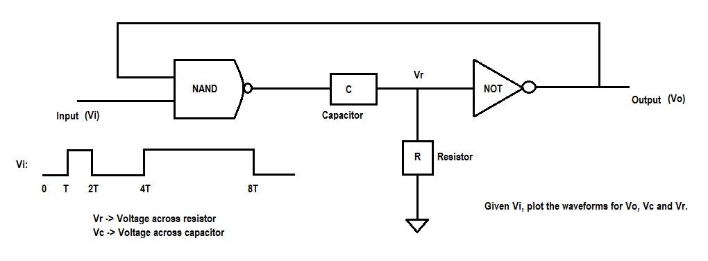
Given is a circuit having a pulsed aperiodic wave pattern, Vi. To be plotted are output waveform Vo, waveform across capacitor Vc and waveform across resistor Vr.
Question 2 can be found at the link given below:
https://picasaweb.google.com/11636060715…
or
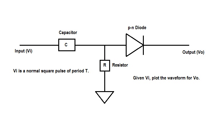
To be found is the output waveform Vo, if the input to the circuit is a uniform square pulsed wave pattern.
While I have been able to almost entirely do Question 2, there seems some very basic conceptual error not leading to the correct answer. As for Question 1, I could find very little headway.
It would certainly not be possible for anyone to plot the waveforms here, and I do not expect anyone to plot the same for me on any other platform. What I require is the method to proceed with these questions and the steps, particularly for Question 1. The required waveforms could be vaguely mentioned in statements, as these answers shall be of utmost help, alongside the methodologies!
I will be extremely thankful to everyone who answers!