Continue to Site

Welcome to EDAboard.com

Welcome to our site! EDAboard.com is an international Electronics Discussion Forum focused on EDA software, circuits, schematics, books, theory, papers, asic, pld, 8051, DSP, Network, RF, Analog Design, PCB, Service Manuals... and a whole lot more! To participate you need to register. Registration is free. Click here to register now.

[SOLVED] ADC conversion problem

Status
Not open for further replies.

syedshan

Advanced Member level 1
Joined
Feb 27, 2012
Messages
463
Helped
27
Reputation
54
Reaction score
26
Trophy points
1,308
Location
Jeonju, South Korea
Activity points
5,134
Dear all,


I am having problem with getting data from my ADC... please see the following

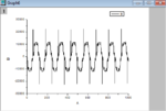
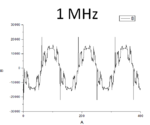
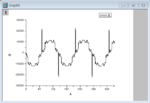
I am giving 125Mhz Sampling clock to1 Mhz Sine wave signal. The image attached is the response that I am getting.

What are these Sudden Jerks or Instant rise or Falls... Is it because of sampling frequency bei

In actual I have to give different signal, but I am having this same Jerks problem with that as well, so I tried it with simple sine wave.
Also When my sampling frequency is 250 Mhz the things are fine...

Please eagerly waiting for response
Capture.PNG
Capture.PNG
 

Looks like data corruption or misinterpretation around zero - what is the ADC?

Keith
 

Thank you for your reply

The ADC is AD62P49.

Looks like data corruption or misinterpretation around zero - what is the ADC?

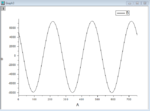
If it were data corruption so it should also be with the 250Mhz sampling frequency. I have attached the figure with 250 Mhz.

Capture.PNG

So I think that is not the case , but if the data corruption is the case then how to avoid it.

The ADC is working with 4DSP board with PCIe communication(4dsp board FM680 board with PCIe communication), so in this case how to reduce data corruption.

Bests,
Shan

- - - Updated - - -

Can sampling clock in any way be the case for this operation, like the accuracy of clock or what is the relation between the signal and the sampling clock's frequency

Bests,
Shan
 

ADC signal problem. Please assist

Dear all,

I am using ADs62p49 ADC from Texas Instrument.

I am having severe trouble in getting PROPER signal from the ADC. Following is the summarized case I tried and result and image

When I tried 250 MHz Sampling frequency I am getting almost correct signal (NOTE: I am giving sine wave as a test wave, 1Khz, 10 & 100 Khz, 1, 5, 10 Mhz)

But when I change the sampling frequency I get completely distorted signals....

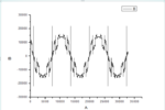
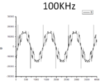
Lets see when I set sampling frequency to 125 MHz I saw the following signals

First is 10 Khz signal
Capture.PNG

Capture.PNG

Capture.PNG

Please help me with this since I have been trying this for about 2 days...

Thanks you in advance.
Bests,
Shan
 

Re: ADC signal problem. Please assist

Looks like incorrect timing in signal processing.
 

Re: ADC signal problem. Please assist

What type of circuit construction are you using for the ADC?

How are you generating a 250MHz clock?
 

Re: ADC signal problem. Please assist

Looks like incorrect timing in signal processing.

I could not understand what do mean by that. please if you can explain it will be easier for me to pick

What type of circuit construction are you using for the ADC?

How are you generating a 250MHz clock?

It is a 4DSP board for Signal processing, I am using internal clock and it I generate 250 MHz and other frequencies using the internal VCO, I am not having slightest of idea what can go wrong if it is working with 250 MHz but not with others.

My actual signal is a sinc wave but even it does not work well with it (i.e. lots and lots of spikes there as well...).

Currently internal construction is like that, VCO generates 1120MHz clock and then I select divider value to generate certain frequencies...

Thank you any way for your response
 

Re: ADC signal problem. Please assist

Than you for your reply


It is FM680 board with FMC104 card (ADC there is ads62p49 and clock distributor embedded inside FMC104)

Bests,
Shan
 

Re: ADC signal problem. Please assist

It could be that one ore more less-significant bits are not working properly. i.e.: one bit is always 1 or 0, or two bits have been swapped. Or even the conversion from 2-complement's has problem (I saw spikes during zero crossing)
 

Looks like the LVDS clock delay is not matching the LVDS data lines. If the part has a phase adjustment on clock try playing with different offsets.

Or if you are running parallel data, same thing, clock not aligned with proper data line same point.

You also need a very low jitter clock for this chip. Less then 0.2 psec which is a very clean clock. Most synthesizers clock chips can't provide this quality.
 
Last edited:
  • Like
Reactions: FvM

    FvM

    Points: 2
    Helpful Answer Positive Rating
I need your full schematic from Analog driver , ADC analog/digital ground isolation, DAC output.
It is clear your noise is independent of the signal input frequency but dependent of sampling clock rate lower than 250MHz.

To me this is analog noise that can come from multiple sources which I can only guess without a schematic.

1. Commutation noise of DAC binary levels adding noise into Analog Vref and output result has quantization noise which changes according to number of bits in transition where biggest is 111111111... to 000000000. I suggest a sawtooth signal to test for linearity and examine Vref noise sources including Analog vs Digital ground.

2. Sample & Hold Commutation feedthru noise Feedthru happens when your source impedance is not low enough to buffer the switch ESR switched capacitance. recommended designs are given in specsheet.

3. Sample and Hold leakage capacitance. I have not used this chip and do not know the sample rate clock sensitivity to clock rate but it appears to me this ADC can only be used at 250MHz with a few pF hold capacitors. the droop causes huge error in holding the input sample. Using a low frequency large triangle wave with a small HF square wave superimposed as a signal source will show how droop changes with level and polarity as a function of ADC sample rate.

Normally ADC's with S&H have external hold capacitor values change according to hold time required for lower sampling rates for a given leakage current. Then successive approx rate (SAR) type ADC's have increasing error as the signal droops on the hold cap.

4. Cross-talk on drooping hold cap from digital states show up as quantization noise.
 
  • Like
Reactions: jasonc2

    jasonc2

    Points: 2
    Helpful Answer Positive Rating
You also need a very low jitter clock for this chip. Less then 0.2 psec which is a very clean clock.
Yes and no. The low jitter clock is required to fully utilize the ADC performance at higher signal frequencies. Usually, only a low jitter crystal oscillator as clock source will give sufficient low jitter, FPGA PLLs and similar "digital" clock sources are missing the jitter requirements by at least one order of magnitude.

But the "trivial" ADC code errors shown in post #1 and #5 are very unlikely related to clock jitter.

I could not understand what do mean by that.
I'm tempted to ask in return: How do you know that the LVDS decoding and succeeding data path timing of your design is correct at all? There are many ways to mix up the ADC data by timing violations in digital design.

I don't believe that the problem has to do with any of the points mentioned by SunnySkyGuy. If I understand right, you are using a ready-made 4DSP ADC daughter board, so the hardware can be expected to be basically O.K.

My suggestion is to activate an ADC test pattern and verify correct data transmission. Adjust the clock phase to the center of the sample window. Define complete timing constraints for the FPGA design.
 
Try do the same measurement with 1/4, 2/4, 3/4, 5/4, 6/4,7/4 off 125MHz clock frequency; and check if the data acquisition clock and adc sampling clock have been changed proportionally. Good luck!
 

The hold capacitor is in pF. with leakage hold time will be in nSec. So it is designed for fast sampling, hence quantization error during successive approximation. If a lower sampling rate is used, the hold time with the analog value, so the Hold Voltage must not change voltage while the analog comparators compare with the Successive Approximate Register SAR design ADC to function correctly.

It is a binary search technique with ADC using a DAC. If analog hold voltage decays to DC neutral, it would be like guessing hi low while the person changes his mind on the unknown number between 0 and 100 while the other person is guessing.

Did you contact TI support as I suggested? What determines the hold time when you change sampling rates?
 
Last edited:

Where do the specs indicate it may operate at any frequency other than 250 MHz ?

Page 6 of the datasheet: 1Ms/s to 80Ms/s in low speed mode, 80Ms/s to 250Ms/s otherwise.

I still think it is a problem of mis-timing in the data read - the problem happens around zero and the size of the problem is huge, so not noise on the analog side.

Keith.
 
  • Like
Reactions: FvM

    FvM

    Points: 2
    Helpful Answer Positive Rating
OK but the noise is what is called quantization noise and the error in SAR comes from noisy V ref crosstalk or droop in the S&H cap

- - - Updated - - -

TY Keith.. It still appears to be quantization noise.. as it is identical for any frequency sine wave being sampled below 250MHz rate.

Just a wild guess but can the input solder joint be broken causing a S&H effect to be ~ 1pF creating this quantization error?
 

Hi all,

I am sorry I started this post and later when I solve the problem I did not post the solution here.

Actually the reason it was corrupted signal was the signal loss as most of you experienced guys correctly said.
Since I was using FPGA integrated with ADC and capturing signals, I have to change the tap delay values at the FPGA
input to get the correct signal.

Hope this might help someone with similar problem.

Bests,
Shan
 

Status
Not open for further replies.

Similar threads

Part and Inventory Search

Welcome to EDABoard.com

Sponsor

Back
Top