Ares6541
Newbie level 1
Hi all,
I have the manufactured PCB in my lab which was designed by myself a week ago. During testing the PCB functionality i came across few problems, which are as follows:
1. The board starts sending in garbage values after operating for five minutes or more.
2. During diagnostics i accidentally put one finger on a part of the PCB and the garbage value was gone. (Sounds weird)
What i am guessing is my board is getting over heated or something and when i put my finger on it the board cools down a bit and shows the actual data to be received.
I have tested it by blowing hot air on that portion of the PCB and the garbage value starts coming and when i put my finger on it after a while i start receiving the actual data.
I am using three AVR contorllers, two on the top and one on the bottom, borad is double layered and the portion which is creating the problem has two capacitors and bunch of vias.
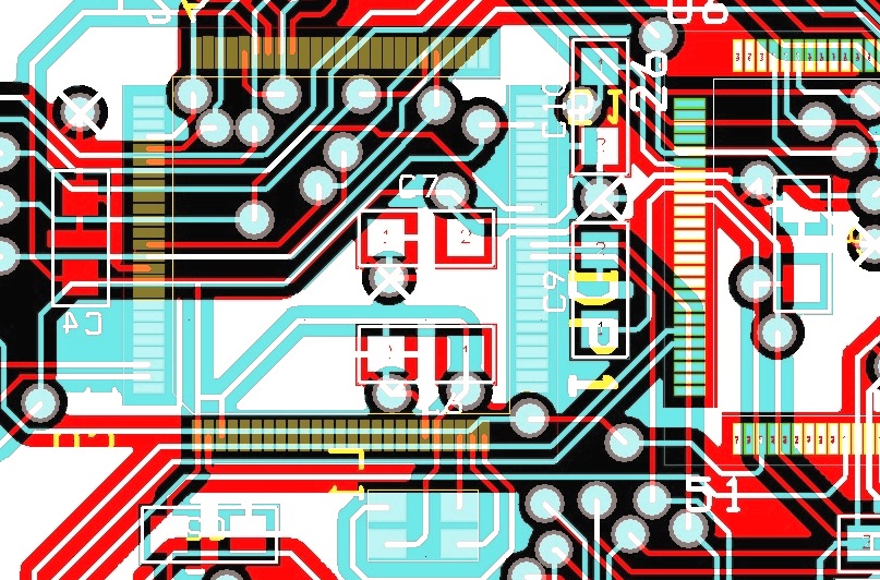
I am also attaching a snapshot of that portion which is creating problem. Its just left of the Two SMD capacitors with a bunch of vias above.

Need your help.
Thanks alot
I have the manufactured PCB in my lab which was designed by myself a week ago. During testing the PCB functionality i came across few problems, which are as follows:
1. The board starts sending in garbage values after operating for five minutes or more.
2. During diagnostics i accidentally put one finger on a part of the PCB and the garbage value was gone. (Sounds weird)
What i am guessing is my board is getting over heated or something and when i put my finger on it the board cools down a bit and shows the actual data to be received.
I have tested it by blowing hot air on that portion of the PCB and the garbage value starts coming and when i put my finger on it after a while i start receiving the actual data.
I am using three AVR contorllers, two on the top and one on the bottom, borad is double layered and the portion which is creating the problem has two capacitors and bunch of vias.
I am also attaching a snapshot of that portion which is creating problem. Its just left of the Two SMD capacitors with a bunch of vias above.
Need your help.
Thanks alot