Continue to Site

Welcome to EDAboard.com

Welcome to our site! EDAboard.com is an international Electronics Discussion Forum focused on EDA software, circuits, schematics, books, theory, papers, asic, pld, 8051, DSP, Network, RF, Analog Design, PCB, Service Manuals... and a whole lot more! To participate you need to register. Registration is free. Click here to register now.

6 layer PCB design issues

Status
Not open for further replies.

sandeep4386

Junior Member level 2
Joined
Feb 1, 2010
Messages
20
Helped
0
Reputation
0
Reaction score
0
Trophy points
1,281
Activity points
1,476
Hello everyone!
I am designing a 6 layer PCB in eagle. I am finished with the routing already. I have few queries and I would highly appreciate if someone could clarify it.

1. I have used a polygon for ground plane and named it as $GND. I have also named all the ground nets as GND. However after creating a polygon and clicking on ratsnest tool, all the ground nets are still not connected to ground plane? Why?

2.After checking for DRC errors, I'm getting 1700 errors!!! Most of them are clearance issues. I can't manually fix all of them. Should I change DRC clearance setting?

3. I routed critical parts manually first and then I tried to use autorouter however it routed all the airwires again and autorouter did not take my manual routing into consideration. What I thought was it would route only the airwires which I din't route manually. Any clue on this???

I have few more questions but I would wait for someone to reply first.

P.S. I have .sch and .brd file for my design. If someone would like to have a look and give me suggestions then I would be more than happy to upload it here.
 

1. Is there a route to the ground plane? In general you must add vias from you component layer grounds with a short track - then the plane layer can connect to the ground net.

2. It sounds like you have been routing with a different set of rules to those set by the DRC. I suggest you edit the DRC rules to suit your PCB manufacturer.

3. I don't use the autorouter so cannot help there.

If you are still stuck the PCB files would be useful.

Keith

I din't quite get ur first point? Are u asking if I have a dedicated layer for a ground plane? Plus, How to add vias from component layer in order to connect ground plane to ground net? Could u elaborate a bit?

I'm attaching .brd file. Please have a look. Thank you for ur help.
 

Attachments

  • Mote_x2.png
    Mote_x2.png
    169.9 KB · Views: 140

I cannot see a brd file - just a screenshot. I cannot see any unconnected nets on there but it is difficult to view. Also, you haven't flooded the ground planes anyway. Maybe if you post the brd file it will be easier to see what is happening.

Keith
 
I cannot see a brd file - just a screenshot. I cannot see any unconnected nets on there but it is difficult to view. Also, you haven't flooded the ground planes anyway. Maybe if you post the brd file it will be easier to see what is happening.

Keith

I connected ground nets manually while routing. However, after adding a ground plane, shouldn't those nets disappear and connect to ground plane automatically?

I tried to attach .brd file but it din't allow me so I uploaded an image file. I have attached .rar file now. You should be able to view .sch and .brd file now.
 

Attachments

  • files.rar
    54.9 KB · Views: 100

I'm also working on minimizing the board dimensions. It would also be very nice of you if you could have a look at component placement and give me some tips if I can make it little more compact.
 
Last edited:

You seem to have a short circuit from your GND pins on two connectors on the right hand side. A 0.1mm track runs right through several pins on the top layer.

You grid is set to 0.001" which seems rather small.

All your tracks are ridiculously small - 0.1mm. Apart from being an unsuitable width for a lot of functions (too small) you will have to pay a premium to get someone to make it.

There are no unconnected grounds after doing a ratsnest. Have you turned on "Ratsnest processes polygons" in the "Set|misc" menu?

Your board edges are not at right angles - probably as a result of using a 0.001" grid for drawing.

For making a break off portion of the board you should use routing (the milling layer on Eagle). Your PCB manufacturer will not make a board with drills like that - the drill will break.

Your DRC errors are probably mostly due to the tracks which are too narrow. Other errors are:


  • short circuits (overlap)

  • drill size
  • drill distance - the break off section mentioned above
  • dimension - items too close to the board edge
  • clearance - tracks too close to other tracks/pads

I would suggest you rip up all the tracks, re-draw the outline with a sensible grid (e.g.1mm), don't use the autorouter, remove the break off holes and then run a DRC. Get a clean DRC before you start. Then set some sensible wire and grid and start manual routing. Run the DRC very regularly to start with and fix errors as you go. That way you will learn and be able to do the DRC less often.

Keith.

Thank you Keith. That was very helpful. I am planning to reroute all the board now. Plus, I Had already turned on "Ratsnest processes polygons" in the "Set|misc" menu. Still GND nets are not getting connected to GND plane. Did that happen when u tried to do ratsnest? In my case, all the ground nets remain the same like I routed them. Wouldn't they disappear and get connected to ground polygon internally?

Also I think I really don't need 6 layers and design can be completed with 4 layers? What's ur thought on this? If I need to assign particular layer to power plane,what all steps I need to follow? In my case I want to dedicate layer 3 to +3.3 V. I never dedicated a particular layer to power plane so far.
 

When I loaded the board & clicked ratsnest it said 'nothing to do'. I also turned off all layers except the ratsnest layer to double check. I will look again tomorrow just to make sure.

Ratsnest with a polygon will not remove GND tracks you have laid down. Normally you wouldn't do any ground or power routing if you were planning to use a power plane except where you need to provide access from a surface mount component to an inner ground (using a via) for example.

You can do power planes in two ways. One is using polygon which you name and can be the whole of a layer. The other is using plane layers which are 'negative' layers. I think it would be safer for you to use polygons. Simply drawn a polygon on the whole of layer 3 and name it the same as the net you want it to connect to. It doesn't matter if the polygon is bigger than the board outline - it will be trimmed to suit the 'dimension' design rule.

I will look at whether it can be 4 layer tomorrow but I would have thought it should be ok.

Keith
 
Well, there are definitely no unrouted nets when I ratsnest. When I load the board initially there are two unrouted traces but they are spurious - they do not end on a component or trace. So, they disappear when I ratsnest. They are probably there because you have deleted some spurious tracking.

By the way, you should also use a sensible grid when placing components - it makes it a lot easier to route.

It should easily route on 4 layers. Even 2 layers is possible but as you should probably have a decent ground plane I would use 4 layers.

One other point on the schematic - you have used a "bus" a few times but as you haven't drawn it going anywhere it doesn't really do anything. Normally buses are used to show a block of connections from one place to another without needing to show the individual nets, which gets messy. You have relied on the net labels for the connections so the bus doesn't show anything. If you want to use a bus then your would run the bus from the radio module to the GPIO connector to show where the connections are going.

You could probably have fitted all the circuit on the first sheet.

Keith.

You are right about the bus. It was redundant and I removed it now. I'm rerouting the board now. I have a component named as MCP1825 which is a voltage regulator and Eagle doesn't have this component listed in its library. What I did is, I went through an online tutorial and made a custom part of my own in eagle library. However I'm not sure whether I created it in a right way or not. I'm especially concerned about the pad positions since there was no information about it in component datasheet. If you get some free time, would that be possible for u to have a look at the package and symbol I made in eagle library. I have a component datasheet too. This is first time I made a new part in eagle library and I don't want to waste manufacturing cost of the PCB if something goes wrong. Please do let me know.

Plus, like I said, I'm rerouting the board. Hence, I might come back to u with some more queries. I really appreciate ur help.
 

I will look later, but one quick check with a footprint is to print it out 1:1 on paper and put the component on it.

Keith.
 

I will look later, but one quick check with a footprint is to print it out 1:1 on paper and put the component on it.

Keith.

Yea that's a nice idea however I don't have component with me. I'm attaching a file with custom library I made and a footprint of a component. Have a quick look at it whenever u have some free time. I'm using DDPAK 5 lead package and u can find package diagram and footprint on page no. 80 and 81 respectively.

I'll get back to u with more queries soon.
 

Attachments

  • MCP1825.rar
    7.5 MB · Views: 82

On the symbol you need to add >name on the name layer and >value on the value layer. If you don't, you won't have the name & value displayed on the schematic.

Also, change the "direction" of each pin to suit the function - they are all I/O at the moment. That will help the DRC work properly.

Normally you would name the pins to suit the function - at the moment you have then named P$1, P$2 etc.

If you look at page 81 of the huuuuge document you attached (for future reference, just link to it - don't upload on here - it wastes server space) it shows the recommended PCB land pattern. Your footprint looks nothing like it. e.g. pad dimensions should be 0.159" x 0.041" max. Yours are 0.066" x 0.032" which seem far too small.

Also, the tab is ground so there should be an extra GND pin on the symbol and a large ground pad on the footprint.

As for the schematic, you need to add >name on the name layer and >value on the value layer.

Don't write MCP1825 on layer 21 - layer 27 is the place for that, but it will automatically be put there if you use the >value on layer 27.

You might want to add a "prefix" to the part such as "IC". Also, you would normally add a "variant name" to match the package type so the suffix ET denotes a 5 pin DDPAK so would be the "variant name" when creating the part.

There are plenty of Eagle tutorials on the net which will cover library component creation.

Keith.
 
Dear Keith,
Thank you very much for all your valuable suggestions so far. I have just finished rerouting the board. I have made quite a few changes in design this time and tried to implement most of your suggestions. I would like to show u my updated design. I'm attaching schematic and board layout file again. Have a look at it in ur free time and do let me know what do u think about it. I'm sure you would have quite a lot of things to add. :)
 

Attachments

  • Files.rar
    54.8 KB · Views: 89

OK.

You have put holes on the milling (route) layer 46 - it should be a rectangle.

Your grid is still tiny - 0.005". I wouldn't normally tun with a primary grid less than around 0.05" on a board like that. The secondary grid can be smaller for tricky routing.

Normally I would use 45 degree routing rather than "all angle". Technically it isn't a problem but it is easier to pack tracks close together if they are at 45 degrees than any angle.

Your defualt track width is 0.016". If you used something like 0.01" then you could pack more tracks in. You would normally use wider ones for power.

I guess you didn't run the DRC as you went. You have a lot of errors:

1. clearance errors - a lot causes by vias touching on the left of the PCB. There are various ways of fixing it - use smaller vias or stagger them (vias are usually wider than tracks).

2. other clearance errors - a lot caused by vias simply touching nearby components or tracks. When switching layers you need to make sure you have enough space to do it. If you notice it is too close then re-do it before moving to the next track.

3. drill size errors - some vias have a 0.01" drill. The minimum drill in your design rules is 0.024". You need to find out what is the minimum you can use with your PCB house.

4. overlap errors - you have tracks crossing pads which have been added to the PCB but not to the schematic so there is no corresponding connection (e.g. across the PCB break-off). Normally you would make sure everything on the PCB is on the schematic.

5. width errors - you have tracks which are 0.007" but the DRC rule is 0.010" minimum

You really need to run DRC as you go and fix the errors as you go. Then you won't spend time routing the whole board to find you have made a mistake on every single track.

Keith.
 

By the way, have you tried the "follow me" router? It is a semi-automatic router which may help you. It will find routes for the tracks as you go and won't put vias and tracks anywhere that design rules would be violated.

Keith.
 

Dear Keith, I have tried to implement all the changes you had suggested to me. It would be great if you could have a look at it again.

You have put holes on the milling (route) layer 46 - it should be a rectangle.
Now its a rectangle. Actually it is a separation of an extension part from main board. I would like to manufacture it in such a way that I can break that part from the main board later on if I want to. I'm not sure if it is a rectangle, how I can break it from the main design?

Your grid is still tiny - 0.005". I wouldn't normally tun with a primary grid less than around 0.05" on a board like that. The secondary grid can be smaller for tricky routing.
If I increase my grid to 0.05" then it wouldn't allow me smooth movement of components and track. Anyways how does grid selection gonna make any difference to design and manufacturing? Isn't grid is only for our convenience?

Your defualt track width is 0.016". If you used something like 0.01" then you could pack more tracks in. You would normally use wider ones for power.
Now default track width is 0.01" and I used 0.015" for power tracks and 0.005" for critical routing.

I guess you didn't run the DRC as you went. You have a lot of errors:

1. clearance errors - a lot causes by vias touching on the left of the PCB. There are various ways of fixing it - use smaller vias or stagger them (vias are usually wider than tracks).

2. other clearance errors - a lot caused by vias simply touching nearby components or tracks. When switching layers you need to make sure you have enough space to do it. If you notice it is too close then re-do it before moving to the next track.

3. drill size errors - some vias have a 0.01" drill. The minimum drill in your design rules is 0.024". You need to find out what is the minimum you can use with your PCB house.

4.
overlap errors - you have tracks crossing pads which have been added to the PCB but not to the schematic so there is no corresponding connection (e.g. across the PCB break-off). Normally you would make sure everything on the PCB is on the schematic.
How can I add these crossing pads in schematic? I dint find any option to add it in schematic.

5. width errors - you have tracks which are 0.007" but the DRC rule is 0.010" minimum

Could you also verify if I have laid down GND and VCC(+3V3) Polygon correctly? I'm little confused about it. Plus, I don't know how to create gerber files for manufacturing 4 layer PCB. It would be of great help if you could guide me about it.

P.S: I have already contacted manufacturer and here are few things he informed me:
Min track width supported:5mil
Min drill:8mil
Min track-track, track-via clearance:5mil.
 

Attachments

  • Files.rar
    55 KB · Views: 92
Last edited:

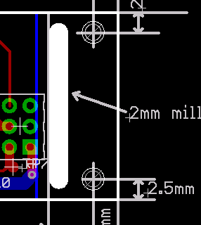
I think you are going to have problems with your break-off. The problem is you have a large amount of remaining PCB because you are running tracks across the break-off. This will make it very difficult to snap off. The PCB company I use route with a 2mm bit so I have usually made a 2mm slot and left a 2mm piece of PCB which is easy to break off:

17_1297417032.gif


I am not sure of the best solution in your case. It depends on why you need the break-off. You could route the tracks through two 3mm pieces of PCB for each connector rather than going straight.

Grid selection is for convenience, but if you make the grid too fine it doesn't help you - you are effectively drawing freehand. A well chose grid will speed up placement and layout. So, if your part legs are on a 0.05" pitch and you want to route 0.01" tracks with 0.01" spacing then 0.05" main grid and 0.01" ALT grid would probably make sense.

You really don't need 5thou tracks for that board. 10thou minimum would be fine.

To make the crossover connections I would suggest you either create a component for the schematic a bit like a connector or add "test pads" to each net you need to connect across the breakoff. You ideally want the schematic to match the layout so you get no errors.

You have other overlap errors which need fixing. You can find them from the DRC.

Your via sizes are strange. 0.01" drill with 0.026" outer diameter. I normally wouldn't go below 0.02" drill on a board like that - there is no need. It pushes the cost up using such small drill sizes and restricts who can make the PCB.

While your power and ground polygons seem to be connected, you haven't made a deliberate connection for them across the break-off.

For generating your output, have a look at the help files or tutorials. There is a gerb274x-4layer.cam job for the cam processor.

Keith.
 

Status
Not open for further replies.

Part and Inventory Search

Welcome to EDABoard.com

Sponsor

Back
Top