EmbdASIC
Member level 5
- Joined
- Feb 18, 2006
- Messages
- 85
- Helped
- 2
- Reputation
- 4
- Reaction score
- 1
- Trophy points
- 1,288
- Location
- Polar Region, Mars
- Activity points
- 1,825
Printing in cadence
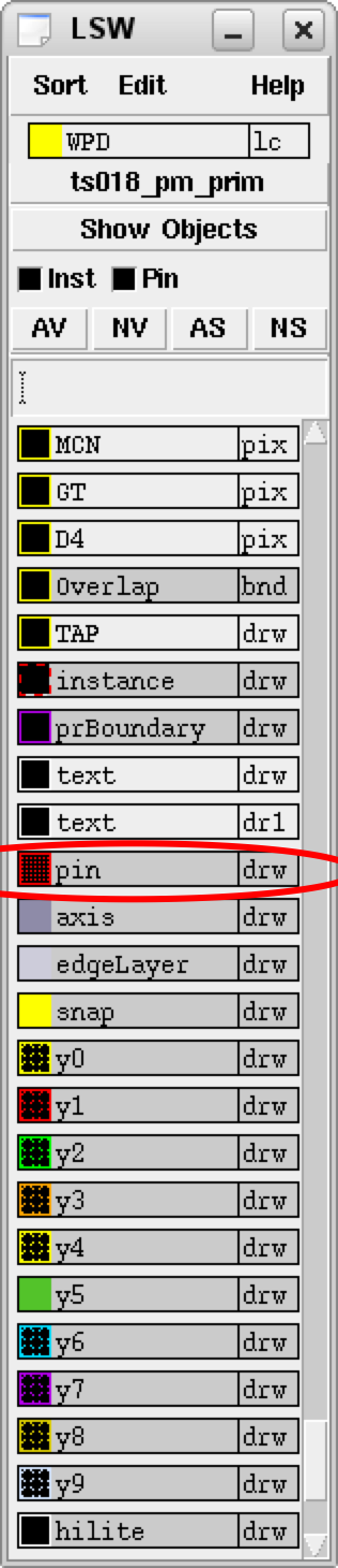
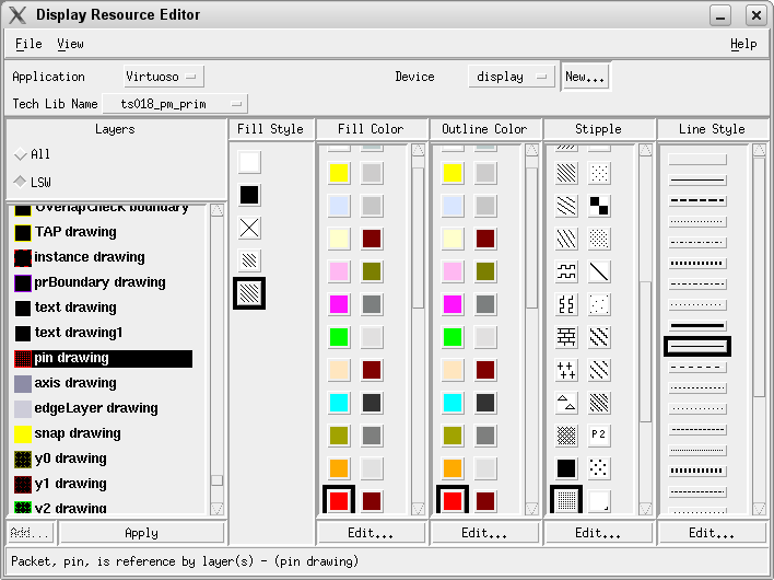
Hello all,
I have something funny to ask!
I want to know if theres any display option with which we can temporarily remove the red square-like terminals of a pmos or nmos instance of a transistor in cadence schematic capture.
Actually it helps in some pretty-printing for documentation purposes !
Thanks you and looking forward for ur suggestions !")
Hello all,
I have something funny to ask!
I want to know if theres any display option with which we can temporarily remove the red square-like terminals of a pmos or nmos instance of a transistor in cadence schematic capture.
Actually it helps in some pretty-printing for documentation purposes !
Thanks you and looking forward for ur suggestions !