Continue to Site

Welcome to EDAboard.com

Welcome to our site! EDAboard.com is an international Electronics Discussion Forum focused on EDA software, circuits, schematics, books, theory, papers, asic, pld, 8051, DSP, Network, RF, Analog Design, PCB, Service Manuals... and a whole lot more! To participate you need to register. Registration is free. Click here to register now.

PA Matching and Bias Design

Status
Not open for further replies.

Julian18

Full Member level 3
Joined
Apr 9, 2007
Messages
167
Helped
5
Reputation
10
Reaction score
5
Trophy points
1,298
Activity points
2,389
Hi, everybody
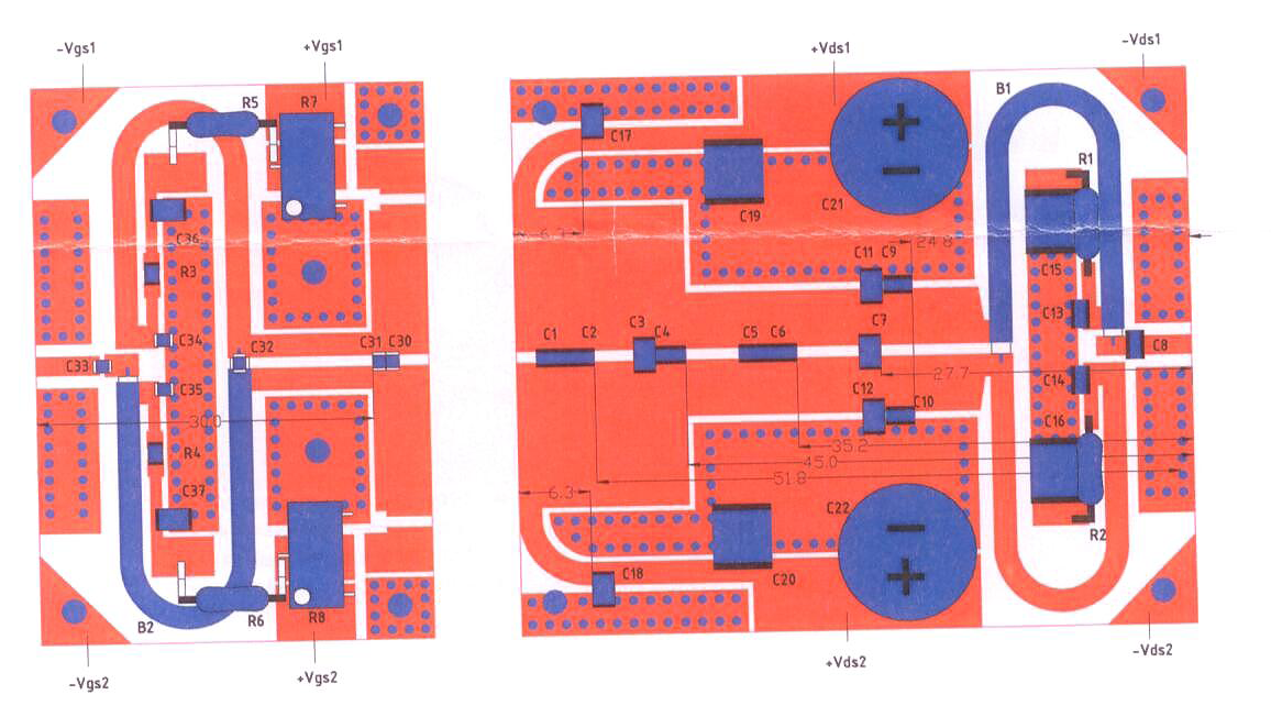
I am a newbie to the area of PA design or more general MW circuit design, although I have a bit of circuit knowledge. Now I am involved in a PA project which uses a NXP LDMOS as the transistor, but I think the circuit is too involved for me. the figure below is the demo circuit shown in the NXP application note.
4166306292_48ec0b9f51_o.png

Now here are my questions:
1. How to design the coaxial baluns at the input and the output.Why do we have to bend it? to save the area or to achieve some other goal?
2. since the balun is "unbalanced", can we erase the microstrip lines? (the micrstrip lines have the same shape as the co-axial balun, only are mirrored around the horizontal line)
3. how to specify the width and length of the matching transmission line? I see a lot of matching networks that are composed of transmission lines paralleled by some caps. but they all have the same width or characteristic impedance. so, why use three section of transmission lines with different width here in the input matching network? for the reason of saying area or some other more fundamental ones?
4. the forth one goes to the biasing network
why does the biasing at the output has round corners connecting to the drain of transistors? to implement inductors? if so , how to design them


Best Regards

Julian
 

I can not see the picture
Please upload it so I can comment.
see following link for designingn Balun
**broken link removed**
You need to study the matching network design to understand how to use stepped matching design.
width will change with characteristics impedance.
It is simple microstrip calculation.
You are saying they have used the network with same width thrice that means the circuit is critical & care has been taken while matching the ciruit so circuit will not oscillate.

upload image again.
 

Hi Abhishekabs
sorry for the unconvenience. I guess now you can see the pics well


Julian
 

why doesn't the pic just show itself instead of being as attachment?

Added after 6 minutes:

try again
23_1260335852.jpg
 

Can you upload the application note?
At first sight the round corners looks like power splitter/devider
 

Hello,
See if you can get any idea about your circuit from the image I have attached.

I got this circuit reference from book
Microwave transistor amplifiers by Gonzalez.
It will be very help ful for you if you refer it.

Tell me if you still have problem.

BR,
Abhishek
 

1. the balun has to be less or equal of 1/8 wavelength at the highest frequency of the intended working frequency bandwidth. In this case it is a 25ohm coax, so it transforms the 50ohm to 12.5ohm at its unbalanced end. Bending is not to save space but to be able to have the opposite curve microstrip line which in effect is an inductor to ground for the inside line/conductor of the coax. It is there to balance the inductor formed by the outside line/conductor of the coax. This is a technique to broaden the work bandwidth and balance both transistors of the push-pull configuration.
2. The above answered this question.
3. You have to learn quite a bit more about matching networks. The series lines of the matching networks are stepped down going towards the lower impedances to be matched. It is a transformer technique again to achieve broadband match and less sensitivity towards tolerances.
4. The biasing lines at the output does not need to be round. In this case they are round just for convenience. The are quite short so are inductances and they part of the matching network also. You don't need additional inductors/chokes in this design.
Hope this helps.
 

    Julian18

    Points: 2
    Helpful Answer Positive Rating
Hi ivanrb
thank you very much for your valuable help. but I dont have a complete understanding about what you've said in ans.1 , so bear for me.

1. I think 25Ohms coax with 1/8 weavelength can only transform 50 to a complex value. i.e. 20-j*15. To goto 12.5 Ohms, we have to use 1/4 wavelength.
as to this broadband technique, could you refer to some readings or references so I can walk it through. As far as I know, this technique is widely used in building PA board, but I failed to find any publication that ever mentioned it.


B.R.

Julian
 

We would need more info to give better answers, but here are some ideas.

It looks like they are i/p & o/p Wilkinson splitters to go from single ended
to differential. I don't know if this needs to be 180° phase shifted or 0°.
If it's 0° you can use resistor combiners/splitters as inputs and outputs.
(The power might be too much for small resistors, more so at the Output).

One main thing you need to understand is that Power Transfer is optimized
when there is a good impedance match. So understand Impedance matching.
Then keep in mind that the best way to get more power is to have low
impedance ! P = V²/Z ! As Z goes down P goes up ! (It might seen contradictory
after you read up on impedance matching (50 Ω systems)).

So for PA's you start ~50Ω match down to (in general) 35-12 Ω PA input -->
PA out (in general) 10-4Ω ---> match 10-4Ω back up to a 50 Ω system!
(Some time you leave the output lower than 50 Ω to get more power).

Note if you only a 5V system ----> Max PWR = V^/Z=5^2/50Ω = 1/2 Watts
OR Max PWR = 5^2/5Ω = 5Watts !

If you DON'T use resistive elements to match you will not loose/dissipate power !

Cheers
 

Status
Not open for further replies.

Similar threads

Part and Inventory Search

Welcome to EDABoard.com

Sponsor

Back
Top