ginebra
Junior Member level 3
Hi Everyone. Happy Holidays. Just want to get some feedback regarding the board layout I made for a 7.9 GHz frequency synthesizer if I did it correctly. The board I am gonna use is a double-sided 1.6mm FR4 board which is why I decided to use microstrip transmission lines in my design.
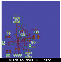
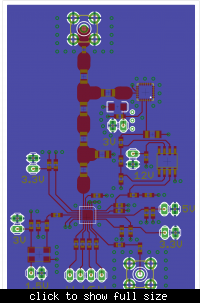
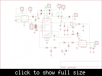
I attached 2 board layouts along with the schematic. One board layout applied the trace width and length calculated from txline while the other board layout has the connections for the 7.9GHz signal path made as short as possible.
This is my first high-frequency board that why I hope to get some feedback to improve my design. Merry Christmas and Thanks in advance.


