Continue to Site

Welcome to EDAboard.com

Welcome to our site! EDAboard.com is an international Electronics Discussion Forum focused on EDA software, circuits, schematics, books, theory, papers, asic, pld, 8051, DSP, Network, RF, Analog Design, PCB, Service Manuals... and a whole lot more! To participate you need to register. Registration is free. Click here to register now.

Best Practices for PCB Design

Status
Not open for further replies.

djsfantasi

Advanced Member level 4
Joined
Mar 14, 2010
Messages
105
Helped
20
Reputation
40
Reaction score
19
Trophy points
1,308
Location
Boston MA
Activity points
1,931
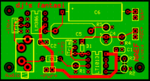
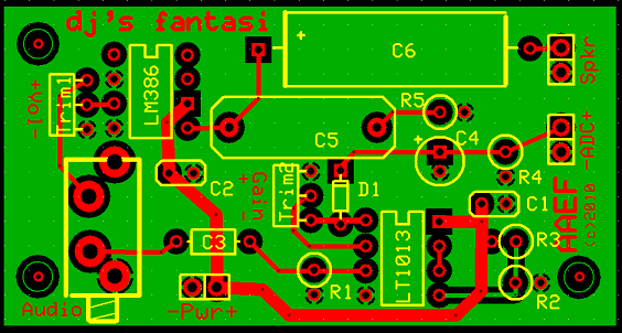
Recently reading the posts about placement of decoupling capacitors as well as looking at other poster's PCB designs, I was hoping someone would comment on my PCB design.

First, I've learned that in the future, I should also include decoupling capacitors at my power input, as well as at each IC. I can also see that I could have placed the capacitor (.1µF) closer to the power connection of the LM386 and with some shuffling of C4, also closer to the LT1013.

Second, I placed circuit traces on the component side wherever possible, soldered on the reverse and the remainder of the solder side was a ground plane. Some of the PCB designs have this reversed. Which side is best for traces?

Could anyone comment on my PCB? I used ExpressPCB, and if you use it, I have attached the final board design (in the zip file) from which I had the PCBs manufactured.

attachment.php
 

Attachments

  • AAEF7b.zip
    27.1 KB · Views: 119
  • aaef7b.png
    aaef7b.png
    95.2 KB · Views: 275

I have had a quick look at your PCB.
I would recommend you make the pads bigger and the dill sockets, The way it is at the moment it might make it harder to make at home, They may get etched away. or if you run the drill through most of the pad will disapear
 
Djsfantasi
Nice looking board, afraid I don’t have ExpressPCB, so haven’t pulled it for a close look.

I think you’ve covered the main points with the decoupling caps.

I’ve seen and routed double sided boards with the ground on top and with it on the bottom, engineers I’ve worked for all have their own preference. With your design, I would prob have flooded the ground on the top layer, so when it’s in your box, your “power” tracks are hidden away under the board, some engineers say it also acts as a ground shield.

I prob would have also flooded the underside of the board with the +5V(?). When you have a pcb with one side full of copper, and the other with only a few tracks, the board will tend to bow as it get hot, something to bear in mind more so if your designing production boards which are wave soldered, or the board in working in temperature extremes.

I would also try to reduce any copper angles less than 90 degrees, these can cause acid traps, which over time can eat away at the copper, with the board failing in the future. Only one I can see is near R3 where it connects to the +5V(?) offset power trace, if the trace runs through the centre of the R3 pad, that would be avoided, maybe at D1 as well.

On your IC’s you have a square pad at for pin 6, and pin 8, normally reserve the square pad to indicate pin 1.

Your text on the copper layers, I would have moved that to the Silkscreen layer, much easier to read. Might also help to indicate polarity on the speaker connector.

Please don’t think I’m picking, main thing to remember, does the board do what you want it to, if it does job done.

Rob
 
Status
Not open for further replies.

Part and Inventory Search

Welcome to EDABoard.com

Sponsor

Back
Top