Continue to Site

Welcome to EDAboard.com

Welcome to our site! EDAboard.com is an international Electronics Discussion Forum focused on EDA software, circuits, schematics, books, theory, papers, asic, pld, 8051, DSP, Network, RF, Analog Design, PCB, Service Manuals... and a whole lot more! To participate you need to register. Registration is free. Click here to register now.

[DSP] 'H1' of TMS320C31 - What is it?

Status
Not open for further replies.

powersys

Advanced Member level 1
Joined
Nov 29, 2005
Messages
439
Helped
3
Reputation
6
Reaction score
2
Trophy points
1,298
Activity points
4,981
tms320c31 dsp,

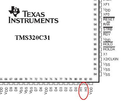
I found 'H1' and 'H3' pins on the TMS320C31 DSP chip. These terms, especially the 'H1', is used frequently in TMS320C31 DSP related user guides. Unfortunately, I have no idea what they are. If I'm not mistaken, it's something to do with 'clock'. Kindly advise. Thanks.

13_1221661943.jpg
 

from page 6 of the datasheet here: **broken link removed**

H1 1 O/Z External H1 clock. H1 has a period equal to twice CLKIN.
H3 1 O/Z External H3 clock. H3 has a period equal to twice CLKIN.

edit to add: from page 6

3. On power up, the processor can be in an indeterminate state. If the state is SHZ mode and H1 and H3 are both held logic high by pull–ups, then shutdown will occur. Normally, if H1 and H3 do not have pull–ups, the rise time lag due to capacitive loading on a tri–state pin is enough to ensure a clean start. However, a slowly rising supply and board leakages to VCC may be enough to cause a bad start. Therefore, a pulldown resistor on either H1 or H3 is recommended for proper wakeup.
 

Do you know the relationships among the following:
[1] Crystal Frequency (say using 50MHz)
[2] Frequency of H1 or H3
[3] Frequency of internal clock connected to timer.

Kindly refering to TMS320C31.

I could not find the info in the user guides.

Thanks.
 

from: **broken link removed**

The clock for the serial port can be supplied externally, or can originate internally through the serial port timer and period registers. The internally generated clock is a divide-down of the clock-out (CLKOUT) frequency, f(H1).

Serial-Port Timing
Although the receive and transmit timers can be configured to be of different rates, it is always a good practice to synchronize both rates to avoid problems. The formula for calculating the frequency of the serial port clock with an internally generated clock depends upon the operation mode of the serial port timers.

If the timer is configured for pulse-mode operation, then:
f(PULSE MODE) = f(TIMER CLOCK) / period register
If the timer is configured for clock-mode operation, then:
f(CLOCK MODE) = f(TIMER CLOCK) / (2 × period register)

Where:

f(TIMER CLOCK) = f(H1) / 2 ; maximum frequency for internally generated clock
f(TIMER CLOCK) < f(H1) / 2.6 ; maximum frequency for externally generated serial-port clock
f(H1) = f(SYSTEM CLOCK) / 2

just a suggestion but a search on google for TMS320C31 will probably prove most helpful. regardless, hope this helps.
 

    powersys

    Points: 2
    Helpful Answer Positive Rating
Thanks. Do you mean the f(system clock) is the frequency of the external crystal (e.g. 50MHz in my case)?
 

If I am reading your question correctly, the answer is yes. I highly recommend downloading the TMS320* User's Guide (Revision F) from:

https://www.ti.com/litv/pdf/spru031f

The guide should clarify the timing aspects you are questioning.

Also I recommend the following:

**broken link removed**

in tinyurl: **broken link removed** if the above link is broken.

The application notes will be of great service, I believe.
 

You are welcome. I'm just glad I could help.
 

Status
Not open for further replies.

Part and Inventory Search

Welcome to EDABoard.com

Sponsor

Back
Top