Continue to Site

Welcome to EDAboard.com

Welcome to our site! EDAboard.com is an international Electronics Discussion Forum focused on EDA software, circuits, schematics, books, theory, papers, asic, pld, 8051, DSP, Network, RF, Analog Design, PCB, Service Manuals... and a whole lot more! To participate you need to register. Registration is free. Click here to register now.

problem with LDO design!

Status
Not open for further replies.
thanks for the response again
it is easy to amplify the error amplifier gain, i can make it reach 70 dB.
concerning the output voltage, that i found, it came from a trans simulation and not a ac simulation.
concerning the compensation, if i reduce only the capacitor in the compensation scheme C1, the stability tend to be enhanced but not so well.so, as adashan said, the dominant pole should come from the compensation scheme and not from the output. in this case, what have i to do? should i increase the output capacitor(2.2µF) or what?

thanks again for all your collaborations.

Added after 2 minutes:

sorry adanshen
i made a mistake when i wrote your name!
 

According to my experience, the dominant pole has not a great influence on the stability margin. Instead you should try to enhance the loop gain phase in the critical region (where the loop gain is app. 0 dB) by adjusting the compensation network.
 

thanks LvW!
i will try to reduce the capacitor C1 and enhance the transconductance of the OTA that is included in the compensation circuitry and i will report you the results.
 

Most probably, adjusting only the value of C1 will not lead to the desired result.
Try also to modify R1 and/or R2 as the resulting time constants are important !
 

hi !
i am trying first to enhance the error amplifier gain but theorically, the gain loop which is l20log(Vb/Va) will decrease if i only enhance the gain of the error amlifier.
an other issue, should i take in account the stability of the error amplifier even before i use the compensation scheme,because you will find reported only the result of the simulation of this amplifier which is obviously not stable at all?
 

imar said:
i am trying first to enhance the error amplifier gain but theorically, the gain loop which is l20log(Vb/Va) will decrease if i only enhance the gain of the error amlifier.

If you enhance the gain of the error amplifier the loop gain decreases ???
This is impossible because the amplifier is part of the loop. Something must be wrong.
Why do you increase the gain of the amplifier up to 70 dB ? That´s more than required and it degrades stability.
Regarding the gain curve you have posted: The amplifier itself is never unstable. It would be unstable if you would use it in a closed loop configuration. However, you are going to use it within a loop consisting of several other parts. Therefore, you have to watch the behaviour of the complete loop - as you have done already by simulating the loop gain (including the compensation circuitry).
My recommendation: Set the gain of the amp to 50 dB, simulate the loop gain for several values of the compensation network and find the best combination which results in a sufficient stability margin.
 

imar said:
hi freinds!
i found some problems duriny=t the design of a Low Dropout Regulator:
this regulator should have: Vdropout:0.5V, so with Vin 3.3V , Vout must be 2.8V.
the load resisttance goes from 28Ω to 2.8KΩ. the Load capacitor is 2.2µF
this regulator has : * a PMOS pass element W=6µ/L=1µ.
* Error amplifier with 60 dB
* bandgap 1.2V
* a frequency compensation scheme


thanks in advance for any response that may help me!

vdrop=0.5V don;t mean vin-vout=0.5V. The output voltage depends on the application. vdrop means the lowest vdd(vin) that could regulate the whole loop to operate normally. for example, If vout = 1.2V, vdrop=0.5V, with this case the minmum vdd(vin)=1.7V. the vdd(vin) must be a voltage range not a specified value as your 3.3V.

In addition, your bandgap output =1.2V, your addtional pole and zero can't be splited with each other adequately
 

hi !
i tried to follow the recommendation, and i fixed the error amplifier gain to the specifed value.so by varying the capacitor value in the compoensation scheme and the only the value of the resistance R2 in the loop, i reached a phase margen of about 48° with an open loop gain of 35dB.
but, when i closed the loop to achieve a trans simulation to find the output voltage, i found that Vout is around 3.2V and not 2.8V which means that the pass element is not working. in fact with a dc simulation, this transistor(W=6m/L=1µ) is in the region 1 i,e Vds< Vdssat and Vgs>Vth.
do the pass element need to be all the time in the saturatin region to keep a drop out voltage(Vrop out=Vds) at 0.5V, and then Vout to 2.8V?
you will find reported the result of the ac simulation of the LDO with RLOAD of 0.75K Ω.

thanks!
 

Firstly if the 35dB loop gain is typical value then I will say its low...

As far as region of operation for pass element is concerned... its good if u can manage to keep it in saturation all the time... but then thats y we define the dropout voltage... after which loop is not in shape to regulate.

Also ,as zhu said you need to specify a range of input voltage and ur desired output voltage... its not like u need to keep the dropout constant ... u need to keep the output constant...

your pass device may go out of saturation... what matters is the total loop gain at that point... if its enough to regulate then no matter if the pass device is in linear or saturation.
 

thanks these new specifications
i am new in designing LDOs and i am trying to understand diffrent points that interfer in this kind of design.
so you said that i should specify a range for the input which is Vdd (Vin).and this point wasn't so clear before.that's why i should use two different voltage sources one for the alimentation of the error amplifier and an other voltage source that will be variable. the question is : how could i fixe this range?
another point: i tried first to maintain the stability for different load resistance value (different load current) for 3.3 V Vin, what should i do now? do i need to run a trans simulation or vary the Vin and watch the ac response?

thanks
 

imar said:
thanks these new specifications
i am new in designing LDOs and i am trying to understand diffrent points that interfer in this kind of design.
so you said that i should specify a range for the input which is Vdd (Vin).and this point wasn't so clear before.that's why i should use two different voltage sources one for the alimentation of the error amplifier and an other voltage source that will be variable. the question is : how could i fixe this range?
another point: i tried first to maintain the stability for different load resistance value (different load current) for 3.3 V Vin, what should i do now? do i need to run a trans simulation or vary the Vin and watch the ac response?

thanks

:D It's ok if it is ur first time.
well you dont need to have two seperate supplies... only one is supposed to be there... the one which you are trying to regulate. Even ur amplifiers and other circuitry is supposed to work on that. The range on which the supply varies itself is a specification.

coming to ur next point regarding the design of ldo...

u first decide the size of ur pass element which shud be able to support the maximum current specified through out the supply range. Then proceed with amplifier design and stability analysis for all the loads(zero to full load) and all PVTs.
and then finaly the GOD ...the transient simulations across PVT.
 

i am afraid, the pass element's W/L is too small, i can not believe W/L =6 can drive out 100mA's current, you'd better re-design it .

by the way , i think you spec is easy realized, if you find your LDO is not stable, you'd better show what compensation you use, where is the domain pole. and please do not use miller compensation, that is not a good idea.
imar said:
hi freinds!
i found some problems duriny=t the design of a Low Dropout Regulator:
this regulator should have: Vdropout:0.5V, so with Vin 3.3V , Vout must be 2.8V.
the load resisttance goes from 28Ω to 2.8KΩ. the Load capacitor is 2.2µF
this regulator has : * a PMOS pass element W=6µ/L=1µ.
* Error amplifier with 60 dB
* bandgap 1.2V
* a frequency compensation scheme
i designed each element apart, and i verified the functionnality of it.
But, when i reessemble the circuit, the circuit goes nice with load resistance of only 2.3KΩ to 2.8KΩ ( current about 1 to 20 mA approximatly).Ifound that Vout is 2.8V and the stability is about 50° as phase margen.
However, if the Rload falls to 1KΩ or less the regulator ceases to work; infact Vout become 3.8V (which means, i think, (Vin)3.3V + (Vdropout)0.5 V) and the circuit is not stable.
is it about the pass element or some thing else?

thanks in advance for any response that may help me!
 

thanks !
first, the pass element hasn't w egal to 6µ but 6m and i rectified it before. it was a taping mistake.
second, THanks Ashish: i have designed my LDO each element seperatly and i fixed the pass element size to W/L to supporte a 100mA to 6m/1µ.
then i designed the error amplifier to have 60 dB dc gain and i used a compenation scheme that i mentioned before.
i have a question: i read that LDO could generate different value of output voltages.is rhat true?
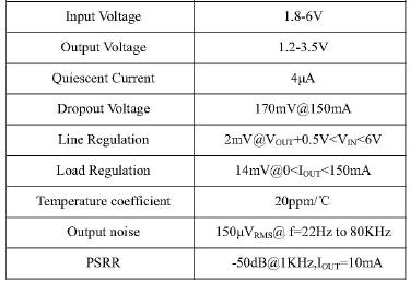
you will find joined a kind of spec. could you explain me what does it mean especially the ranges of Vin and Vout?
how could i achieve a PSRR simulation in Cadenec and how could i found the quiescent current?
thanks a lot for yr help.

Added after 3 minutes:

31_1219645818.jpg
 

plz refer to the attachment for the spec defination of LDO.
 

    imar

    Points: 2
    Helpful Answer Positive Rating
imar said:
thanks !
first, the pass element hasn't w egal to 6µ but 6m and i rectified it before. it was a taping mistake.
second, THanks Ashish: i have designed my LDO each element seperatly and i fixed the pass element size to W/L to supporte a 100mA to 6m/1µ.
then i designed the error amplifier to have 60 dB dc gain and i used a compenation scheme that i mentioned before.
i have a question: i read that LDO could generate different value of output voltages.is rhat true?
you will find joined a kind of spec. could you explain me what does it mean especially the ranges of Vin and Vout?
how could i achieve a PSRR simulation in Cadenec and how could i found the quiescent current?
thanks a lot for yr help.

Added after 3 minutes:

31_1219645818.jpg

Well firstly, the documents that zhu has uploaded ae really good enough to understand what those specs are...

coming to ur questions explicitly...

yes there are ldos which can provide different output voltages.... but not at same time :D

u can make ur ldo programmable by programming the uppe resistence of ur feedback ladder. The verification in this case has to exhaustive as u are trying to change the feedback factor .

taking ur specs as a case : the regulator can work on a range of input supply varying between 1.8 to 6v.
this regulator can be progrramed to give a minimum o/p voltage of 1.2 volts upto 3.5 volts. NOTE the output has to stick to one value throughout the supply range and load range. It is not like vout cna be anything between 1.2 to3.5 .

say once programed for 1.2 volts o/p ... it has to give 1.2 volts for all values of vin between 1.8 to 6v.

Coming to PSRR simulations... its simple to run ... just add a ac voltage to ur Input votage, set the output load to 10mA and raun ac simulations as in normal course. the value of vout /vin in decibles gives ur psrr.

next the quesient current... just run a transeint simulation with nolaod condition and note the current consumption.... thats ur quescient current or ground current.
which in ur spec is 4uA...

hope this helped to some extent...

do mention if u need some help further
 

    imar

    Points: 2
    Helpful Answer Positive Rating
thanks for all these information!
let's look now to another point, when i tried to simulate the dc open loop gain with AC simulation for different Rload values the phase alternate its origine and when i reduce RLOAD , it begun from 180° and not from 0°, which means that inputs V+ and V- of the error amplifier are not stable?
how can i manage to resolve with this problem?
 

you are urself answering ur question... if it is unstable... then stablize it... work on the compensation... see what is the location of ur system poles and zeros...
then accordingly design a compensation network.
 

imar said:
thanks for all these information!
let's look now to another point, when i tried to simulate the dc open loop gain with AC simulation for different Rload values the phase alternate its origine and when i reduce RLOAD , it begun from 180° and not from 0°, which means that inputs V+ and V- of the error amplifier are not stable?
how can i manage to resolve with this problem?

You should try to express yourself as clear as possible - otherwise you cannot expect some help from outside.
1) AC analysis for simulation of DC open loop gain sounds confusing
2) What do you mean with "open loop gain" ? (Probably "loop gain", the term "open loop gain" normally is used for amplifiers alone)
3) What do you theoretically expect for the phase response ? Start at zero deg. ?
4) Inputs cannot be stable/instable

Recommendation: Post both response curves which confuse you.
 

1/2- for the AC analysis, i meant the loop gain but the term 'open' was added to show that this simulation was runned with an open loop.
3- to have a stable system the phase margen us calculating referring to 180°. so i think that the phase has to begin from 0. if it is not the phase margen could be around several degrees 100° or even more as the corves shown.
4- concerning inputs, you have right. i only want to say that V+ and V- alternate and not a stability issue of inputs.
 

imar said:
1/2- for the AC analysis, i meant the loop gain but the term 'open' was added to show that this simulation was runned with an open loop.
3- to have a stable system the phase margen us calculating referring to 180°. so i think that the phase has to begin from 0. if it is not the phase margen could be around several degrees 100° or even more as the corves shown.
4- concerning inputs, you have right. i only want to say that V+ and V- alternate and not a stability issue of inputs.

- The phrase "loop gain" always means "open" - otherwise it makes no sense since there is no input/output of the loop.

- Each stable system with negative feedback has a loop gain phase of -180 deg for low frequencies (if the minus sign within the loop is taken into account; in control systems, sometimes only the black boxes are considered without the minus sign).

- That means, only your display in the middle looks OK.

- IMPORTANT: You can NOT trust ac analysis for unstable systems. It looks as everything would be OK, but it isn´t. Both of your displays with zero deg phase shift for low frequencies indicate INSTABILITY. You can check this by doing a tran analysis which certainly show that the system does not work properly.
(As a simple example, an ac analysis for an opamp with positive feedback would give results which looks pretty good).

- Resumme: You have to adjust the compensation network to stabilize the loop for lower load resistances.
 

Status
Not open for further replies.

Similar threads

Part and Inventory Search

Welcome to EDABoard.com

Sponsor

Back
Top