Continue to Site

Welcome to EDAboard.com

Welcome to our site! EDAboard.com is an international Electronics Discussion Forum focused on EDA software, circuits, schematics, books, theory, papers, asic, pld, 8051, DSP, Network, RF, Analog Design, PCB, Service Manuals... and a whole lot more! To participate you need to register. Registration is free. Click here to register now.

Help needed on VHDL code.

Status
Not open for further replies.

kokei74

Junior Member level 3
Joined
Apr 2, 2008
Messages
30
Helped
0
Reputation
0
Reaction score
0
Trophy points
1,286
Activity points
1,528
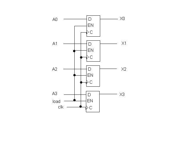
hi, im quite new to VHDL and currently is learning now. I try to create a D flip flop with enable from a D flip flop using a port map.

48_1216784104.jpg


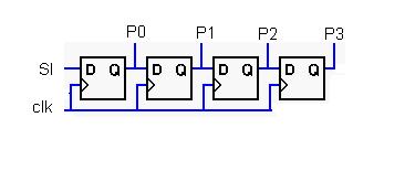
here is VHDL for DFF

library ieee;
use ieee.std_logic_1164.all;

entity dfflop is
port (D,clock :IN std_logic;
Q :OUT std_logic);
end dfflop;

architecture logic of dfflop is
begin
process (clock)
begin
if clock'event AND clock = '1' THEN
Q <= D;
end if;
end process;
end logic;


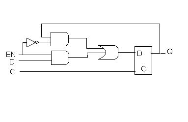
Here is VHDL for DFF with enable.

library ieee;
use ieee.std_logic_1164.all;

entity DFF_en is
port (EN,D0,C :IN std_logic;
Q0 :OUT std_logic);

end DFF_en;

architecture logic of DFF_en is
signal p0 : std_logic;

component dfflop
port (D,clock :IN std_logic;
Q :OUT std_logic);
end component;

begin

p0 <= (NOT EN AND Q0)OR(EN AND D0);

stage0 : dfflop port map (p0,C,Q0);

end logic;

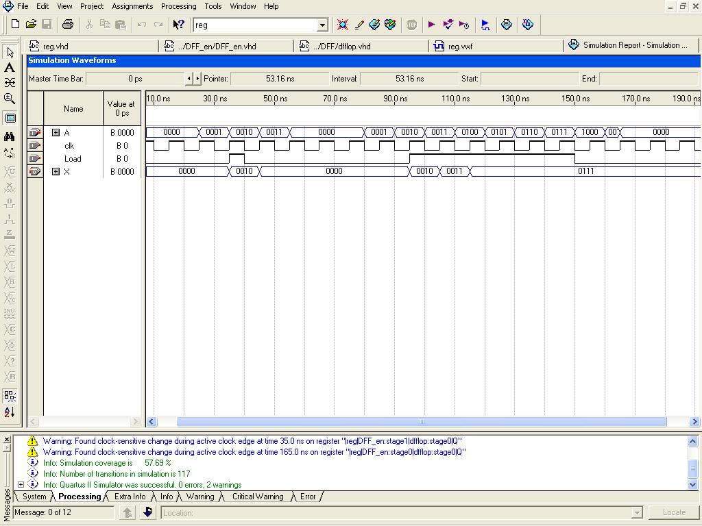
when start compilation this error occur.
Error: VHDL Interface Declaration error in DFF_en.vhd(21): interface object "Q0" of mode out cannot be read. Change object mode to buffer or inout.
Error: Ignored construct logic at DFF_en.vhd(11) because of previous errors

Please help me verify what is the problem. Thx
 

You are getting this error because you are trying to read the output port Qo which is not permitted .
Solve this by defining an internal signal...below is the code.

Code:
library ieee;
use ieee.std_logic_1164.all;

entity DFF_en is
	port	(EN,D0,C		:IN std_logic;
				Q0		:OUT std_logic);
				
end DFF_en;

architecture logic of DFF_en is
signal p0 : std_logic;
signal Q0_int :std_logic;

	component dfflop
		port	(D,clock :IN std_logic;
				 Q		 :OUT std_logic);
	end component;

begin

p0 <= (NOT EN AND Q0_int)OR(EN AND D0);

stage0 : dfflop port map (p0,C,Q0_int);
Q0 <= Q0_int;
end logic;
 

i tried to used ur code but error still occur.

Error: Net "Q0~0", which fans out to "Q0", cannot be assigned more than one value
Error: Net is fed by "comb~0"
Error: Net is fed by "dfflop:stage0|Q"

what thus that mean?
 

i had forgotten to change the Q0 to Q0_int in port map... i think it should work now..
 

its work fine. Thx a lot. :D

but maybe i will need ur help again. Ater this i want to combine this Dff to create a register. :D
 

hi again..
suppose when EN = 1 the the data on 4 input is transfer into the register with the next positive clock edge. when EN = 0 the current value remains in the register at the next positive clock edge. So EN will determine whether the next pulse accepts new information or leave the information in the register . From my simulation why does the output 0100, 0101, 0110 did`t come out after 0011 but it skip to 0111 and suppose when EN = 0 after that it should preserve 0111 until the next positive clock edge.


simulation result


VHDL for register

library ieee;
use ieee.std_logic_1164.all;

entity reg is

port ( A :IN std_logic_vector (3 downto 0);
Load,clk :IN std_logic;
X :OUT std_logic_vector (3 downto 0));

end reg;

architecture logic of reg is

component DFF_en
port (EN,D0,C :IN std_logic;
Q0 :OUT std_logic);
end component;

begin

stage0 : DFF_en port map ( A(0),Load,clk,X(0));
stage1 : DFF_en port map ( A(1),Load,clk,X(1));
stage2 : DFF_en port map ( A(2),Load,clk,X(2));
stage3 : DFF_en port map ( A(3),Load,clk,X(3));

end logic;
 

Ok...! in your port map you have mapped load as D0 input to all DFF...it should be A instead....
it is better to use named port mapping association to get a better insight in the beginning of vhdl experiments....
 

for port map can u tell me how does the input position?

stage0 : DFF_en port map ( A(0),Load,clk,X(0));
1st 2nd 3rd 4th

how to arrange input 1,2,3,4?

btw what didt u mean by "named port mapping association"?
 

stage0:dff_en port map
(EN => load,
D0 => A(0),
C => clk,
Q0 => X(0));


and so on....
this is what is called as named association and the one you are using is positional association...
 

i see.. now its work correctly as i wan. thx :D

using this name associate is much more easy for beginner..

can help me create a serial-parallel and parallel-serial register using this DFF?
a block diagram maybe so i can work on the VHDL code.

Added after 1 hours 3 minutes:

this is for my serial - parallel register

14_1216974722.jpg


VHDL code

library ieee;
use ieee.std_logic_1164.all;

entity regsp is

port ( SI :IN std_logic_vector (3 downto 0);
Load,clk :IN std_logic;
P :OUT std_logic_vector (3 downto 0));

end regsp;

architecture logic of regsp is
signal s0 : std_logic;
signal s1 : std_logic;
signal s2 : std_logic;

component dfflop
port (D,clock :IN std_logic;
Q :OUT std_logic);
end component;

begin

stage0 : dfflop port map (D =>SI,clock=>clk,Q=> s0);
stage1 : dfflop port map (D =>s0,clock=>clk,Q=> s1);
stage2 : dfflop port map (D =>s1,clock=>clk,Q=> s2);
stage3 : dfflop port map (D =>s2,clock=>clk,Q=> P(3));

P(0)<=s0;
P(1)<=s1;
P(2)<=s2;

end logic;

got some error for my serial input logic type. Suppose for serial input it is like 1100 then for declaration it should be SI :IN std_logic_vector (3 downto 0)??
 

There are many good books and other resources are available for basics of digital and vhdl.....you should refer to them . Get a fpga board and start experimenting with it.
If you face any problem this forum can help you...
Happy coding.
 

Hi!

Change

Code:
SI	 :IN std_logic_vector (3 downto 0);
to

Code:
SI	 :IN std_logic;

But for best result in future follow kvingle advices!
 

    kokei74

    Points: 2
    Helpful Answer Positive Rating
serial input should be single bit and not a vector.
 

    kokei74

    Points: 2
    Helpful Answer Positive Rating
yes yes just now confuse about serial input. now understand alrdy. :D
btw thx for ur help. I surely need to study more about VHDL. :D

Added after 20 minutes:

Hi, can u suggest the best FPGA board for me?
i think i will need 1 for my future project.
 

kokei74 said:
yes yes just now confuse about serial input. now understand alrdy. :D
btw thx for ur help. I surely need to study more about VHDL. :D

Added after 20 minutes:

Hi, can u suggest the best FPGA board for me?
i think i will need 1 for my future project.

Hello

There are lot of Dev. Board. For right choice you need to solve some questions.

1) FPGA/CPLD Vendor
2) Target FPGA/CPLD
3) Board End Market (DSP/Automotive/Communication/Storadge etc.)

For beginer - see cheap entry level CPLD board.
(for example **broken link removed**)

But if you have a tons of money see this
https://www.dinigroup.com/DN9000k10.php :D


-- Good Luck!
 

Status
Not open for further replies.

Part and Inventory Search

Welcome to EDABoard.com

Sponsor

Back
Top