Continue to Site

Welcome to EDAboard.com

Welcome to our site! EDAboard.com is an international Electronics Discussion Forum focused on EDA software, circuits, schematics, books, theory, papers, asic, pld, 8051, DSP, Network, RF, Analog Design, PCB, Service Manuals... and a whole lot more! To participate you need to register. Registration is free. Click here to register now.

RF common source MOSFET amplifier

Status
Not open for further replies.

I14R10

Full Member level 3
Joined
May 31, 2015
Messages
185
Helped
0
Reputation
0
Reaction score
0
Trophy points
1,296
Activity points
2,750
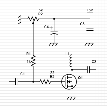
I need some help with the calculations for common source MOSFET amplifier. I want to design RF preamplifier for 50W RF amplifier. I decided to go with MOSFET. I came across this schematics


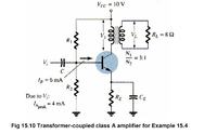
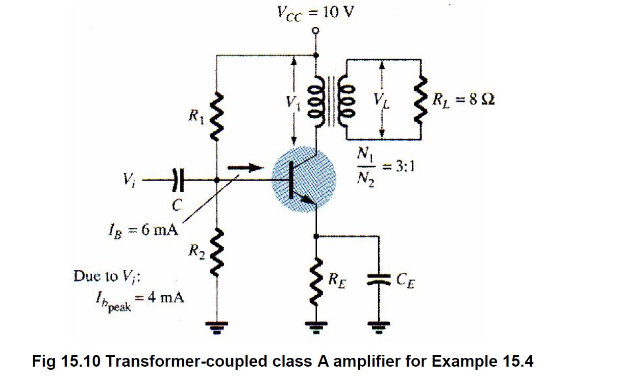
It's for BJTs, but I tried to replace BJT with MOSFET. With IRF510 https://www.futurlec.com/Transistors/IRF510.shtml
To keep it simple I removed source resistor and capacitor. So we just have that transformer in the drain.
I will first write what I calculated and then ask the questions.

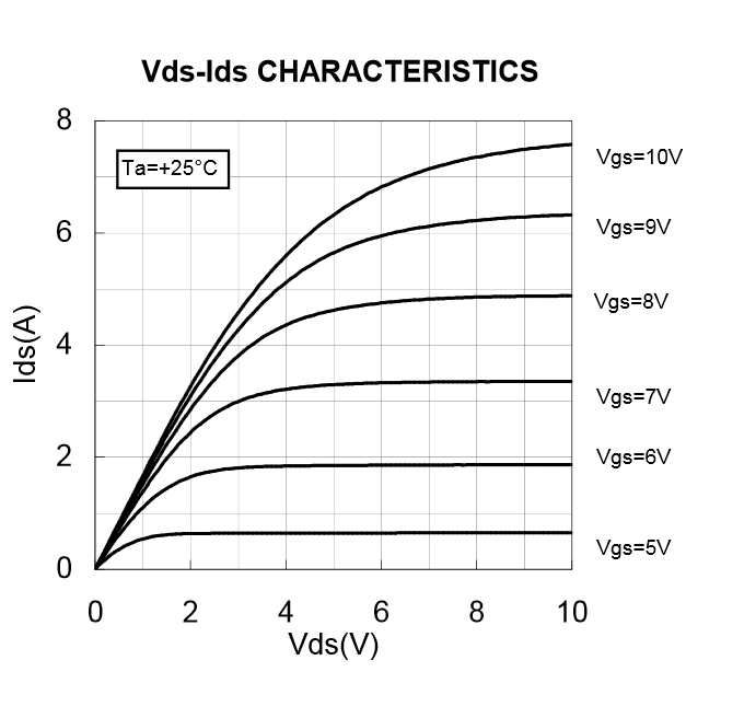
R=Vdd/Id=30/4=7.5 ohm. That is maximum resistance that should appear on transformer to allow Id=4A. I chose Id=4A because the transconductance curve was the most linear around 4A
. Instead of using R(load)=8ohm, I am using 50 ohms. That means that turn ratio should be 1:2.6 (drain : load). Now I have a load of 7.5 ohms across transformer primary coil.


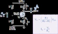
Next I calculated R1 and R2 to set up gate bias. R1=225k, R2=50k. That gives Vgs around 6.6V. And If you look at the datasheet that is the voltage needed to give Id=4A with Vdd=30V.

Does this calculations make sense?
--------------------------------------------------------------------------------------

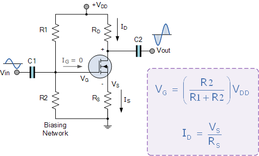
Now if we put back source resistor, here is what I am doing

I said earlier that maximum Rd should be 7.5 ohms. Now that we have source resistor, we should take for example, Rd=6.5 and Rs=1 ohm.

Rd=6.5ohm
Rs=1ohm
Id=4A
---------------------
For no signal, the primary transformer coil on the drain is short circuit, Rd=0ohm.
But if there is a signal then Rd=6.5ohm (with 50 ohm load on secondary coil)

Vd=Id*Rd=26V
Vs=4V
--------------------
Vds=22V

We have to adjust gate bias to be 10.6V so that Vgs=6.6V

From datasheet, the transconductance is 2S. That would get gain of 13 for amplifier with source resistor and gain of 14 without source resistor.

Can somebody confirm these calculations and my comments?
 

This is not the way to design an RF power amplifier. The Impedance seen by the drain is related to output power and useable supply voltage.
The source should be directly grounded and the bias set according to the operating class of the amplifier. I would suggest AB rather than A.
I don't have time to go through all the steps required but to make a successful amplifier, even in the low tens of watts takes a lot of care.
The IRF510 is not designed for RF amplifer service but some can be made to deliver power up to low VHF and is considerably cheaper than an RF device.
The following links are the result of just a few momenttes searching for Fet RF power amplifier design. They should get you started.

www.golddredgervideo.com/kc0wox/wa2ebyamp/amppart1.pdf
www.golddredgervideo.com/kc0wox/wa2ebyamp/amppart2.pdf
www.nxp.com/documents/handbook/RF_Fundamentals.pdf
www.dtic.mil/dtic/tr/fulltext/u2/a258384.pdf
www.qsl.net/va3iul/Bias/Bias_Circuits_for_RF_Devices.pdf
www.qsl.net/va3iul/RF_Power_Amplifiers/RF_Power_Amplifiers.pdf

Peter
 

Sorry, this doesn't help me. I read through them, as well as other 20 papers. I better start building circuits in real life. I won't learn anything only by reading books.
 

Motorola published some good application notes and engineering bulletins by Helge Granberg, they may be around 30 years old, but many are very practical and contain most if not all of what is needed to design a working amplifier.
This site, **broken link removed** seems to have quite a few of the ANs. Search for motorola rf amplifier application notes and or Helge Granberg.

NXP ( Philips ) used to have some good ap notes too, not so sure about what they have now though.

The basic procedure is to match 50 ohms to the impedance that the device needs to see to todeliver the power you want with the supply voltage you have, then match 50 ohms to the input impedance of the device. Setting the bias comes towards the end when adjusting for best linearity and standing power consumption.

If you just want to build an amplifier then you could do worse than copy the one in the first link in my last post.

Peter
 
  • Like
Reactions: I14R10

    I14R10

    Points: 2
    Helpful Answer Positive Rating
Have a look at the design for 'pennywhistle' a broadband HF driver amp capable of 10 - 20W from the HPSDR project, it is fairly typical of the sort of thing you want.

IRF510 will be nothing but pain until you gain much more understanding, RD16HVF1 and friends will be much better behaved (Less parasitic source inductance apart from anything else).

Start by calculating the voltage you need across the load, this and the supply voltage give you a good start on the drain match (transformer or L match depending on how much bandwidth you need), then swamp the gate until the ting stops trying to take off and match into that for the drive.

You need temperature compensated bias as the fet will tend to thermal runaway.

I **Highly** recommend a copy of 'experimental methods in RF design', well worth the time.

73 Dan.
 
  • Like
Reactions: I14R10

    I14R10

    Points: 2
    Helpful Answer Positive Rating
I will certainly buy that book. In the meantime I managed to correctly calculate values for the amplifier. I checked it in electronics workbench and it worked. Just to explain to you - I don't plan to design big amplifier, I know that is a problem. I just need 2W of power to feed it to amplifier that I plan to build, from a schematic that works.

Do you have any idea how to measure the signal voltage without oscilloscope? We will see if my transmitter will work, but if it should work, I need to know the signal voltage after a mixer and IF amplifier. Only than I can complete my calculations for this amplifier.
 

The MOSFET IRF510 can use a simple voltage divider for gate bias. For just 2W output power you don't need smart bias scheme. Very important for these kind of MOSFETs is the bias decoupling network and its grounding designed on the PCB layout, otherwise the transistor get unstable. Don't forget to isolate the drain from the heath-sink.
Set initial for low DC bias current and increase the idle current until you get the desired linearity of the transistor.

 
  • Like
Reactions: I14R10

    I14R10

    Points: 2
    Helpful Answer Positive Rating
Just one quick question -this is a screenshot from rd16HH1 datasheet


I tried calculating, for Id=0.6A few different load impedances. It seemed that if I choose bigger load impedance that I would have greater voltage swing and more power developed on the load.

For example, for load impedance of 300 ohms I get current of 100mA (Vdd is 30V), that means 100mA in positive and 100mA in negative direction. The voltage developed on that load is +/-30V with input voltage of 100mV. I took that from datasheet. That equals to 1.5W of power on the load.

Is this correct?

It's strange, at first I thought that I need large current to get more power on the load, but it seems that I need small current and large voltage to get more power.
 
Last edited:

Can somebody please answer me

For example I choose operating point for MOSFET at Id=0.6A, Vgs=5V. I put transformer in the drain that transformes 50 ohms impedance on secondary to 300 ohms impedance on primary. That means that current through the primary coil is 0.1A. So how can current Id=0.6A flow through the MOSFET? It should be 0.1A. Unless we look at the DC and AC component separately.
 

The AC and DC are separate.
The FET sees a DC drain resistance of a fraction of an ohm, ideally 0ohms. The AC component sees the transformed load impedance which is one of the components setting the gain of the circuit.
Work out what current is needed in the load for the power you need and set the DC bias accordingly.
Search for Transformer coupled class a amplifier There is a lot of information out there, mainly aimed at audio ampifiers I expect, but the basics are the same.
 
  • Like
Reactions: I14R10

    I14R10

    Points: 2
    Helpful Answer Positive Rating
I did search and I already calculated. I didn't quite understand this with separate AC and DC current. Thank you.
 

Status
Not open for further replies.

Part and Inventory Search

Welcome to EDABoard.com

Sponsor

Back
Top