Continue to Site

Welcome to EDAboard.com

Welcome to our site! EDAboard.com is an international Electronics Discussion Forum focused on EDA software, circuits, schematics, books, theory, papers, asic, pld, 8051, DSP, Network, RF, Analog Design, PCB, Service Manuals... and a whole lot more! To participate you need to register. Registration is free. Click here to register now.

Bandgap voltage reference and voltage level issue

Status
Not open for further replies.

AMSA84

Advanced Member level 2
Joined
Aug 24, 2010
Messages
577
Helped
8
Reputation
16
Reaction score
8
Trophy points
1,298
Location
Iberian Peninsula
Activity points
6,178
Hi guys,

I would like to know which type of circuit one can use to produce a voltage higher than 1.2V but still with the same temperature dependence shape?

Regards.
 

Most current-mode BGVRs can achieve reference voltage >1.2V. The most well-known one is: A CMOS bandgap reference circuit with sub-1-V operation, JSSC, May 1999.

Hi guys,

I would like to know which type of circuit one can use to produce a voltage higher than 1.2V but still with the same temperature dependence shape?

Regards.
 

This is just a bandgap reference with a buffer amp,
and whatever feedback ratio you want. Similarly a
bandgap with post-divider and amp, will give you a
lower VREF (have done this on several POL DC-DC
designs). Only problems are if you insist to do it in
an extremely low transistor count, or at a total supply
headroom below 1.5V or so. Otherwise, hang an op
amp and couple of resistors off the back (or use the
amp that's already there in the bandgap, if it's the
diodes-and-op-amp type already) and you're there.
 

Thanks for the input.

This voltage reference is to be done for a DC DC converter, mainly to the sawtooth generator where we need to have the reference voltage in one of the two pins of the op-amp that is used to set the threshold voltage.

@mohmohcha, I'll try that circuit. I'll read the paper.

@freebird, sorry for the inconvenience, but I didn't got the point.
 

@mohmohcha, I tried the circuit that you have suggested and I am facing some problems.

I have designed that circuit using a single-stage diff. amp and a start-up circuit.

While running corners (3V only), I got this strange behavior from the circuit:

bandgap.png

When I run simulation he has that strange behavior. Does anyone know what might happening? It has something to do with the startup circuit? Or the diff amp?
 

If you doubt it is the start-up circuit problem, check the operating regions of the transistors and voltage at different nodes at the temperature not working.

Better analyze the problems a bit first before asking, this is one of the most important things for engineers.

Another possibility is the stability of the system; the amplifier introduces another pole and forms a feedback loop, you may need to add a capacitor to the amplifier output for compensation. More details can be found in Jacob Baker's book.


@mohmohcha, I tried the circuit that you have suggested and I am facing some problems.

I have designed that circuit using a single-stage diff. amp and a start-up circuit.

While running corners (3V only), I got this strange behavior from the circuit:

View attachment 113455

When I run simulation he has that strange behavior. Does anyone know what might happening? It has something to do with the startup circuit? Or the diff amp?
 
  • Like
Reactions: AMSA84

    AMSA84

    Points: 2
    Helpful Answer Positive Rating
You were right mohmohcha. However, after reviewing the circuit I concluded that I had a bad connection in one of the transistors.

That said, there is something that is confusing me: The circuit right now is operating ok. Producing a nice output current with a very small error. But what is confusing me is this:

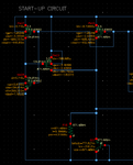
start.png

It is normal to have a current around 700uA in the transistor that is at the middle of the start up circuit?

SIZES: Up left - 2/2um; middle 10/1um; down left 10/50um.

Regards.
 

Use minimum width for transistors on the left hand side, and set the length of the nmos as long as possible depends on your layout.

You many want to use cascode current mirror also. Can already imagine your circuit has large line regulation. Just found an interesting paper and you can find some tips there. Lee et. al., "A Sub-μW Bandgap Reference Circuit With an Inherent Curvature-Compensation Property", TCAS1, Jan 2015.

You were right mohmohcha. However, after reviewing the circuit I concluded that I had a bad connection in one of the transistors.

That said, there is something that is confusing me: The circuit right now is operating ok. Producing a nice output current with a very small error. But what is confusing me is this:

View attachment 113466

It is normal to have a current around 700uA in the transistor that is at the middle of the start up circuit?

SIZES: Up left - 2/2um; middle 10/1um; down left 10/50um.

Regards.
 
  • Like
Reactions: AMSA84

    AMSA84

    Points: 2
    Helpful Answer Positive Rating
Hi mohmohcha. I managed to put the circuit working. However, I have a doubt here: It is suppose to have the upper left transistor in the same size of the other? (In Baker's book he uses all the upper transistors with the same width, includingm in this case the upper left transistor)

For all effect, that upper left transistor is a current mirror, right? So I can use a different size to achieve a different current (less than the reference I want) in a way that will make the start-up circuit work.

Am I right?

Thanks in advance. Regards.
 

That pmos transistor is not part of the current mirror, and is only a pull-up device. The idea is that, after the BGVR starts up, PM27 sets the gate voltage to of PM23 to VDD. As a result, PM23 is off and draws no current.
 
  • Like
Reactions: AMSA84

    AMSA84

    Points: 2
    Helpful Answer Positive Rating
Hi, thanks. Well, but who sets the voltage isn't the NMOS NM28?

Regards.
 
Last edited:

The BGVG has two operating regions, either idle (not sure if this is the correct work) or working.

In idle mode (before the BGVR starts up), all the nodes' voltage is either 0 or VDD; the gate voltage of NM28 is VDD. As a result, PM23 is turned on and the BGVR starts up.

The gate voltage of NM28 decreases until PM27 (has a much larger driving than NM28) is turned on and turns PM23 off. The BGVR then functions normally.
 
  • Like
Reactions: AMSA84

    AMSA84

    Points: 2
    Helpful Answer Positive Rating
Okay.

mohmohcha, one more thing.

I have noticed that in some simulations the following happens: When I ask for the output current, cadence gives the expected curve almost independet of temperature. However, the DC parameters or DC op point doesn't match with what the plot is giving. For example, in the output transistor the current that appears next to the mosfet is in the order of nA but the output curve gives something around 10uA.

This can be a bug from cadence? Or is something that I am doing wrong? Which one should I trust?

NOTE: There are some other curves that I have obtained that both matched in some way.

Regards

- - - Updated - - -

I forgot to tell that this issue happens when, for example, I have the PTAT resistor (the one in the 8 BJT branch) from the analogLib and a susbst. this resistor for an RNHR1000 with the same value, which has a third terminal that is connected to VDD.
 

Don't think this is Cadance's problem and my experience tells me not to suspect the simulator. Show me your DC simulation settings and the schematic, otherwise I can't help.

I always suggest people to do hand calculations before designing, then you usually know if you are on track.
 

Here you go:

here_you go.png

- - - Updated - - -

I noticed that this happens when, for example, after running the temperature sweep, I do a VDD sweep and the result is the 1uA at the end of the sweep (@3.3V -> 1uA) and all the nodes are updated with different values when compared to the temperature sweep.

That's way I ask if it is a bug.
 

Clearly, your amplifier is driving pA current and not working. The VBE of the npn transistors is 70mV, what are you expecting actually? And where is the compensation capacitor? It seems to me that you change the start-up circuit, and I suppose it is not working also.

Again, I suggest you to do hand calculations first; don't think you can get a good design if you keep doing this.
 
Last edited:

Thanks for the reply. I ask, what kind of hand calculations? To implement the start-up cricuit? I haven't found any kind of literature reference on how to do this. The rest is simple.

However, even though, as you say, that the circuit is driving a pA current, I got that output plot. So if the circuit is driving a pA current how do I have an output curve?

Regarding the compensation capacitor, I didn't understood for what that is needed, because the amplifier, this one is competly stable and moreover, I don't know the value that the capacitor should have because never found in any paper any reference to the value of that capacitor. Moreover, I tried the compensation capacitor (because I thought too that the result could be because of the lack of the compensation capacitor) and nothing happened. I tried several values.

Kind regards and thank you in advance for taking some of your time to try help me out how to understand this.

EDIT: I forgot to say another thing. I managed to put the circuit working (producing the reasonable amount of current - say 10uA i each BJT branch) with some current in each BJT branch and have a nice compensation output current. However the problem comes when running corners, specially when varying the resistance corners. What is funny is that every paper that I read with more or less attention they never showed their corners result taking into account the resistance variation.
 
Last edited:

Thanks for the reply. I ask, what kind of hand calculations? To implement the start-up cricuit? I haven't found any kind of literature reference on how to do this. The rest is simple.

- I meant the calculation of the output current.

However, even though, as you say, that the circuit is driving a pA current, I got that output plot. So if the circuit is driving a pA current how do I have an output curve?

- In the last schematics you showed, the VBE of the BJTs are 70mV and the id of NM13 is 30pA.

Regarding the compensation capacitor, I didn't understood for what that is needed, because the amplifier, this one is competly stable and moreover, I don't know the value that the capacitor should have because never found in any paper any reference to the value of that capacitor. Moreover, I tried the compensation capacitor (because I thought too that the result could be because of the lack of the compensation capacitor) and nothing happened. I tried several values.

- The amplifier is stable, but it forms a feedback loop with more than one pole when you add the amplifier to the BGVR. Because the transistors are with similar sizes, people usually add compensation capacitors (see Baker's book).

Kind regards and thank you in advance for taking some of your time to try help me out how to understand this.

EDIT: I forgot to say another thing. I managed to put the circuit working (producing the reasonable amount of current - say 10uA i each BJT branch) with some current in each BJT branch and have a nice compensation output current. However the problem comes when running corners, specially when varying the resistance corners. What is funny is that every paper that I read with more or less attention they never showed their corners result taking into account the resistance variation.

- The output current varies with the resistor corners, but the output voltage does not. The variations of the resistors (same material) cancel out if you do a good layout.
 
Last edited:

mohmohcha thanks for the quick reply.

Well, the output current calculation doesn't have much to say.

My comment is this:

However, even though, as you say, that the circuit is driving a pA current, I got that output plot. So if the circuit is driving a pA current how do I have an output curve?

- In the last schematics you showed, the VBE of the BJTs are 70mV and the id of NM13 is 30pA.

If you notice in the picture, there is a curve plot. That curve plot was taken from the output transistor (the one with the resistor in series - ideal one). While the circuit is showing those results pA, mV and stuff, I manage to have an ouput curve as you can see in the picture.

I don't get it. Do you understand what I mean?

How do you explain I have all that stuff indication in the circuit and have an ouput current plot as you can see?
 

This is your circuit and no one can debug your circuit better than you do. If you insist this a a bug from Cadence, I think you better email them.

What I can say is I don't see a normal start-up circuit in your last schematics. I don't think I have more comments to add.

Remember to do the transient simulations also. Good luck!
 
Last edited:

Status
Not open for further replies.

Part and Inventory Search

Welcome to EDABoard.com

Sponsor

Back
Top