Continue to Site

Welcome to EDAboard.com

Welcome to our site! EDAboard.com is an international Electronics Discussion Forum focused on EDA software, circuits, schematics, books, theory, papers, asic, pld, 8051, DSP, Network, RF, Analog Design, PCB, Service Manuals... and a whole lot more! To participate you need to register. Registration is free. Click here to register now.

Power Amplifier Circuit Diagram Problem

Status
Not open for further replies.

TheAntiDoctor

Junior Member level 2
Joined
Feb 9, 2014
Messages
20
Helped
0
Reputation
0
Reaction score
0
Trophy points
1
Activity points
184
Hi Everyone,

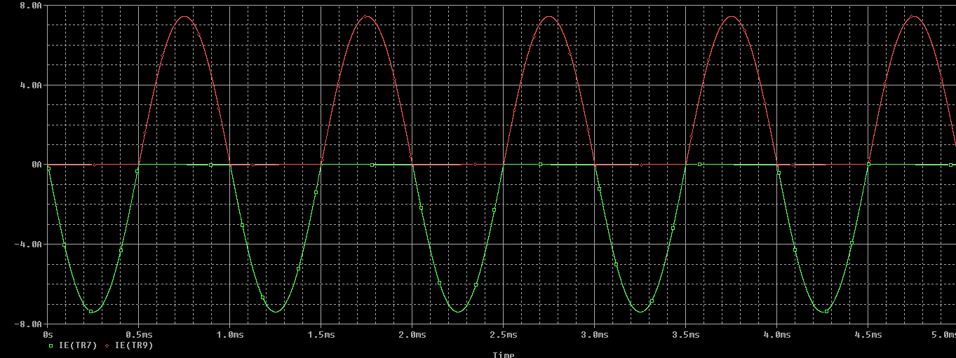
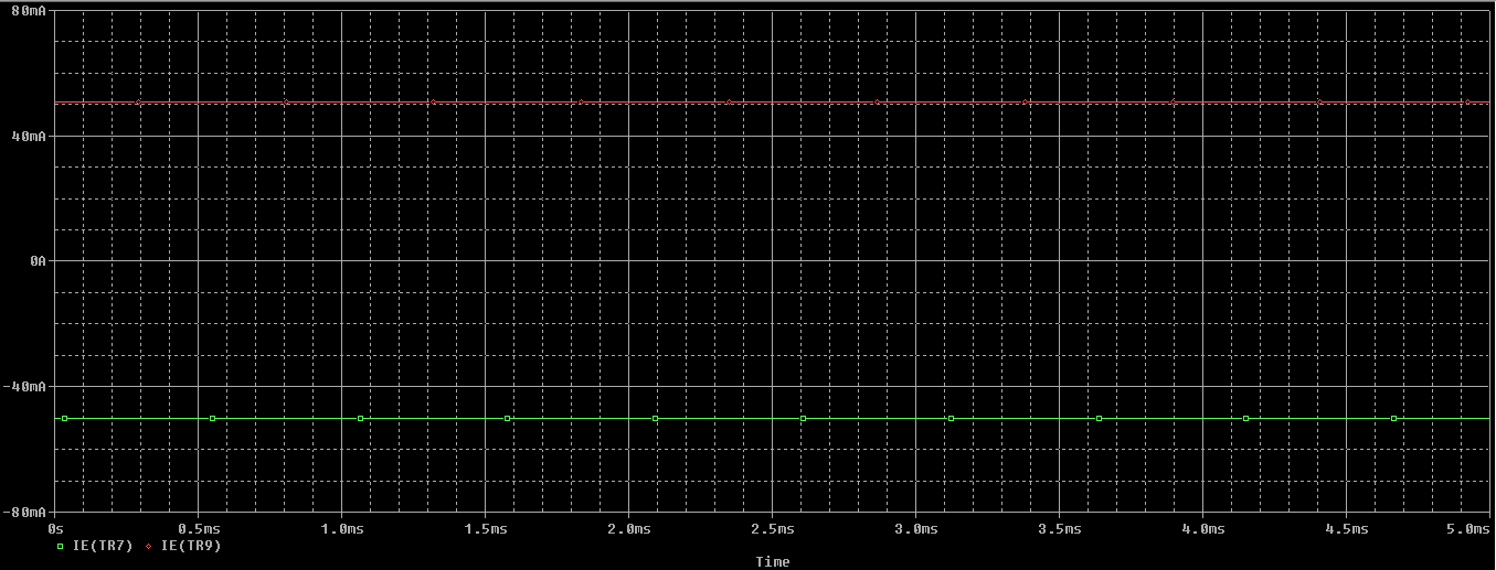
Thanks a lot for checking out my post, I really appreciate any help you can provide. I have been tasked with creating a blameless power supply, which is what I've done, according to the attached schematic. However the output doesn't match what the output should be by a long way.

I have a feeling I have made a mistake with the input of the schematic (How do I represent the NFB?) also PR1 is just a variable resistor that I've replaced with a regular resistor.

I have included my schematic, a copy of the output and a copy of what the output should be based on what I've been told, any pointers would be really appreciated, many thanks :)
Current Diagram.pngpower transistor current.pngschematic original.pngSetup requirements.png
 

Looks like there is another NFB node at the output of the original schematic. Try connecting the NFB at the input to the NFB at the output.

Also, I do not see any DC power in the simulation? The +/-37VDC?
 
Last edited:

Looks like there is another NFB node at the output of the original schematic. Try connecting the NFB at the input to the NFB at the output.

Also, I do not see any DC power in the simulation? The +/-37VDC?

Thanks for the reply!

I'll have a go with the NFB link as soon as I can. I assumed that the + and -37V power suggested an AC power supply at the input rather than 2 separate DC voltage supplies located elsewhere?
 

The text on the original schematic says, "Class-B Amplifier" which is wrong. It is class-AB.

I agree that the simulated amplifier will work much better when it has a power supply (+ 37V and - 37V) and has the negative feedback (NFB) connected.
The audio input says, "VAMPL = 37V" which must be another error.
 

Thanks for the reply :) So the AC input I have on at the moment at 37V and 1kHz frequency isn't working as a power supply? What should the input be then if the DC power supply is located somewhere else?
 

Your AC source on the input is just the input signal and not power. 37VAC will be too large but you will see this when you get things running. Add + and - 37VDC supplies reference to 0V/Ground where shown on the original schematic.
 
Thanks a lot, I'll get that going as soon as possible and let you know the results, thanks a lot for the help, it's really appreciated!!
 

The amplifier has a signal voltage gain of (R8/R9) +1= 21 times. With a power supply that is +37VDC and -37VDC its maximum output peak voltages are about 32V so the maximum peak input signal is 32V/21= 1.5V which is 1.08V RMS. I do not know if your simulation uses peak or RMS signal voltages.
 

The text on the original schematic says, "Class-B Amplifier" which is wrong. It is class-AB.

I am just about to start work on this again today, what makes you say that this amplifier is class AB and not just B? The schematic I received is apparently an excerpt from the guy who literally wrote the book on blameless power amplifier design, Douglas Self, so I would have hoped it would be a reliable source!
 

I don't believe that class AB versus class B is the problem here. Some authors are simply subsuming class AB under class B if the bias current is very low.

Presently you need to figure out some much more basic points, e.g. why an audio amplifier needs a power supply, what is amplifier gain, how do you use an amplifier at all? After that there's time to look for subtile nuances in your books.
 

It's just slightly sloppy terminology. If there's no quiescent current in the output transistors, then it's a class B amplifier. When you adjust the trimpot so that there's some quiescent current in the output transistors, then it's a class AB amplifier.

When you get the simulation working, you can fiddle with the value of the trimpot (or the resistor you replaced it with), and see how it affects the quiescent current.

edit: Oops, cross-post with FvM.

- - - Updated - - -

Also:
I have been tasked with creating a blameless power supply...
It's an amplifier, not a power supply. The idea is to connect a low-level audio signal from e.g. an MP3 player to the input, and connect a loudspeaker to the output.

It does need a power supply though, hence the +-37V supply connections on the schematic.

The two points marked "nfb" on the original schematic should simply be connected together.
 

The amplifier uses Motorola transistors that I used 50 years ago. It was the "blameless" amplifier designed by Douglas Self: https://www.eetimes.com/document.asp?doc_id=1274885&page_number=4 . In the article he says the quiescent current was a little low to completely eliminate crossover distortion spikes so maybe that was why he called it class-B.

It produces 50W into 8 ohms, not 4 ohms and its distortion was very low (0.001%).
 
Presently you need to figure out some much more basic points, e.g. why an audio amplifier needs a power supply, what is amplifier gain, how do you use an amplifier at all? After that there's time to look for subtile nuances in your books.

I am aware of the basic facts about amplifiers in general, specific audio amplifiers are new to me. An audio amplifier needs a power supply for obvious reasons - you don't get an amplified signal for nothing, you need power for the amplifying circuit to work. An amplifier's gain is its capability to increase the amplitude or power of a signal or a specific ratio of input to output. An amplifier is obviously used to increase a weaker signal for a wide variety of applications, such as those used in MP3 players or homes sound systems.

All of this and more I am used to as theory and basic principles but as I'm sure any person is aware of knowing facts and putting them into practice is a very different matter. Combined with trying to get to grips with the less than intuitive interface of PSpice and OrCad Cadence and the whole thing can get lost very quickly! Thank you for reminding me that basic principles are still the most important.

- - - Updated - - -

Thanks for echoing the suggestions of others, I can't understand why they didn't just connect the two nfb points together though as you would in a normal schematic?
 

I can't understand why they didn't just connect the two nfb points together though as you would in a normal schematic?
Doing it this way is arguably a bit neater. What you don't want is a long line weaving around all over the schematic, which would be hard to follow.
 

Hi everyone,

So, thanks to all your help, which I will reference at the end of this report, I have changed the circuit diagram appropriately. I have also changed the input voltage as specified in a part of the report to 1.414V, equivalent to RMS 1V. The output is much improved! All is well however the report specifies that the output current from TR7 and TR9 needs to be manipulated to create between 48 and 52mA. This is meant to be done by changing the value of the variable resistor, now PR1 however when I change this resistance value the output current doesn't change at all, any help would be greatly appreciated!


The idea is to set the DC current to about 50mA, when there's no input signal.

FWIW, I'm surprised he specified 50mA. The optimum setting for minimum distortion would be higher - probably about 100mA, as explained on his website, in his books etc.
 

So, I have set the input to 0 and altered the variable resistor PR1 to adjust the output current to allow the emitter voltage from the transistors to be approximately 50mA. However the current from both emitters is not strictly measured as +50mA, one is positive and the other is negative. I'm assuming this is okay however and due to the negative and positive voltage supplies, since they are both relative to these power supplies the current is effectively positive on both?

Now to do the actual 12 questions, I'm going to need some caffeine for this and a lot of patience!


Now you have a nice amplifier BUT your load is only 4 ohms which might overload and overheat the output transistors. The article I posted about this amplifier has an 8 ohm load for an output of 50W.
 

Hey everyone,

I've been working through some of the questions for this amplifier and so far it's been going well, however, now I've been tasked with measuring the high and low power bandwidths. I know what bandwidth is but I am having troubles where and what exactly I should measure, if you guys could point me in the right direction that would be great. The full questions are attached


- - - Updated - - -

Now you have a nice amplifier BUT your load is only 4 ohms which might overload and overheat the output transistors. The article I posted about this amplifier has an 8 ohm load for an output of 50W.

Thanks a lot for the reply :) The question paper actually specifies a 4 ohm output for the circuit and that it is looking to drive 110W into a 4 ohm load
 

I've been working through some of the questions for this amplifier and so far it's been going well, however, now I've been tasked with measuring the high and low power bandwidths. I know what bandwidth is but I am having troubles where and what exactly I should measure, if you guys could point me in the right direction that would be great. The full questions are attached
The parts listed have their functions described in the design article of this amplifier I posted.
R27 and C6 are not a filter. They are a zobel network. It provides a low impedance load at high frequencies where a loudspeaker becomes a high impedance due to its inductance. When the load on the amplifier is high at high frequencies then inductance or capacitance at its output might cause oscillation.

R19 and L1 prevent a capacitive load from causing the amplifier to oscillate. A speaker with a crossover network becomes capacitive near its crossover frequency. The cable connecting the amplifier to a speaker has capacitance. R19 reduces the Q of L1 to prevent ringing.

I think all these parts do not affect the low power frequency response of the amplifier.
It is easy to measure the low frequency and high frequency -3dB points. EDIT: An audio amplifier is not measured up to 10GHz. I think this one is -3db at 80kHz that you cannot see on your very wide range of frequencies.

The question paper actually specifies a 4 ohm output for the circuit and that it is looking to drive 110W into a 4 ohm load
Maybe you should mention in your answer that this "blameless" amplifier was designed for 50W into 8 ohms and might be overloaded and might overheat with 110W into 4 ohms.
 

Status
Not open for further replies.

Part and Inventory Search

Welcome to EDABoard.com

Sponsor

Back
Top