Continue to Site

Welcome to EDAboard.com

Welcome to our site! EDAboard.com is an international Electronics Discussion Forum focused on EDA software, circuits, schematics, books, theory, papers, asic, pld, 8051, DSP, Network, RF, Analog Design, PCB, Service Manuals... and a whole lot more! To participate you need to register. Registration is free. Click here to register now.

Continous Sigma Delta ADC- Choosing the proper DAC

Status
Not open for further replies.
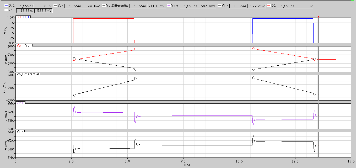
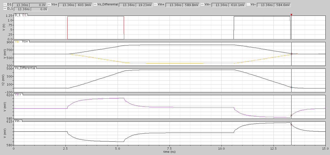
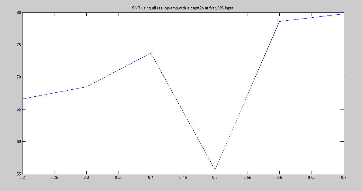
first, the problem I see is, you put a step pulse to your integrator, therefore, it should integrate with a slow due to the current and the C. Since you have feedback around your amplifier, this should result in the summation node staying at VDD/2 with only a small ripple. If its moving like what you have, you need to find out why... If you put in an ideal amplifier again, does it do the same thing?? Do this to check.

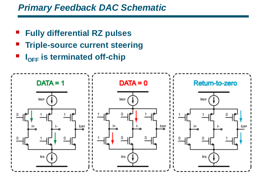
second, is your DAC a current steering DAC or a switched resistor DAC? If its a current steering DAC NO resistors are there, just two cells. If its a switched resistor DAC you should have 2 resistors in each cell for a 1.5Bit switching.. then you would need reference voltages.

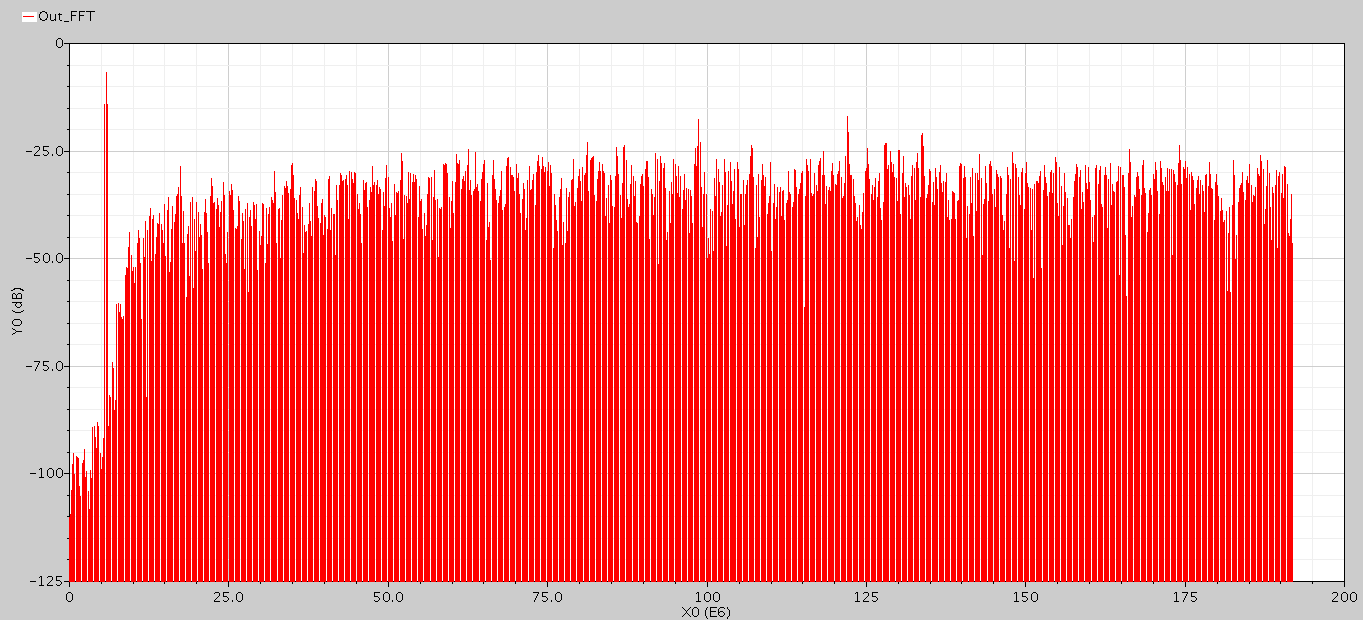
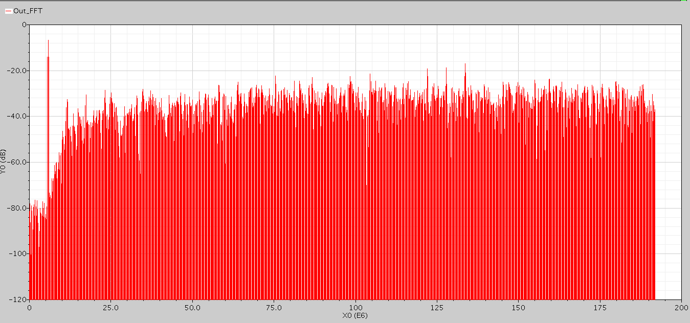
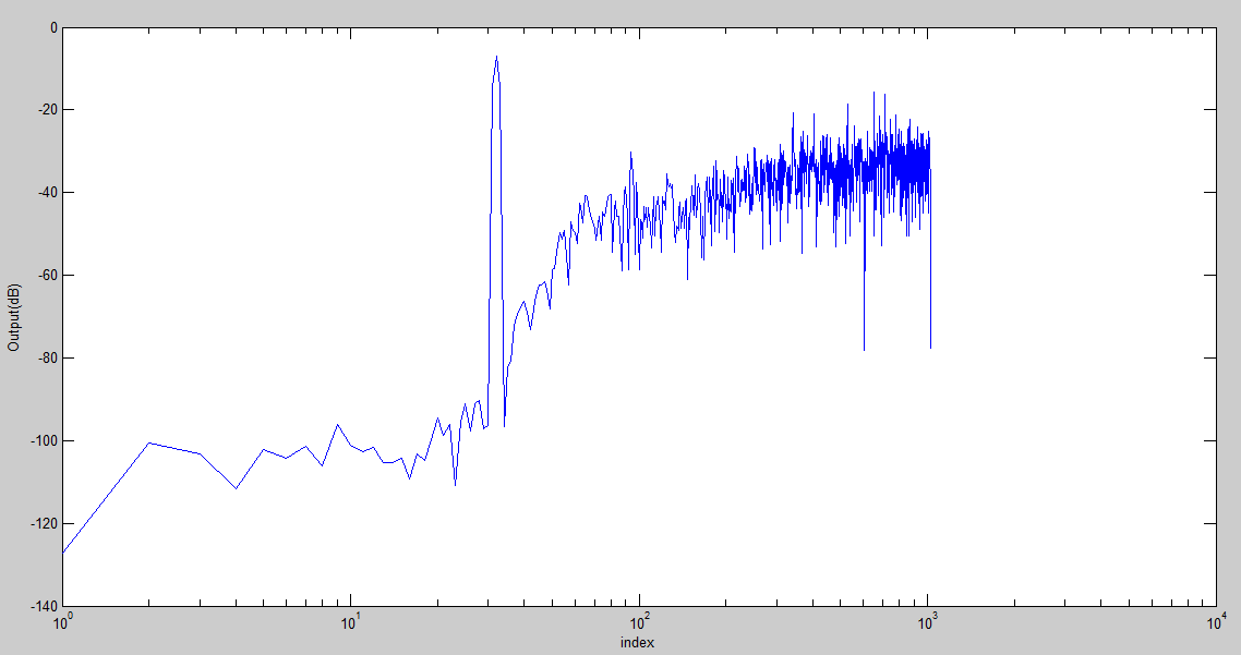
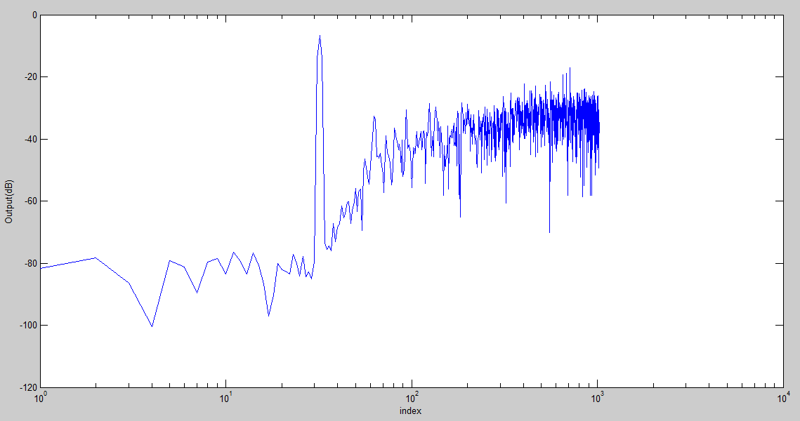
Last, as for testing your DAC you need to test it in your entire ADC with all other blocks being verilogA modeled.. I know it takes time but that is the hard part about designing DSMs. If you have a DAC in place, switching a ~380MHz, I would say like 4 hours for a good spectrum. If you include the amplifier maybe another 2 hours. Trust me this is still short. When you finish the entire ADC and simulate with parasitics it can take easily 4 days to a week!!!!!

JGK
 
With your virtual ground voltage going to supply, clearly your opamp is not working. With an ideal opamp, what is the swing at the output of the integrator? How have you chosen R and C values.? Have you ensured that the swing at the integrator output is such that opamp can support it? How is the waveform at vo_l2 and vo_r2 look like ( not just the differntial output ). ? Can M10, M11,M12 and M3 still remain in saturation when the voltages at vo_l2 and vo_r2 reaches it max (min)?
Replace your opamp with an ideal opamp (as JGK said). See the voltage swings at each node and whether an actual opamp will be able to support it. If not, you need to properly scale R and C.
 
How have you chosen R and C values.?

I tried changing the value of R & C with keeping the time constant as it is.

When i changed the C into 0.1p , (instead of 4p), Vin+ & Vin- changes between 580mV & 620mV , which is much better.

i didn't choose the previous value carefully, as i thought that what's important is the ratio only, i didn't know that value of C would affect the performance greatly.

Based on what should i choose the values of R & C ??

Thanks for your help.
 

You can't just change your R to C values (keeping the ratio the same) while not changing the DAC current!!!!!! This changes your input feed-in coefficient and your feedback coefficient which should be equal (unless you are doing STF changing in the passband)!! First you choose your input R to meet your thermal noise requirements, then you calculate your C, lets say here, your coefficient is 0.5, therefore your C = 1/0.5*fs*R. <-- the 0.5 is your coefficient. This sets your time constant to what you want to design. Next what is your full scale swing..... Lets say it is +-300mV, then you take your input 300mV/R=full scale current which your DAC will provide(single side since its fully differential). Then since you have a 1.5bit DAC cell that means each cell's current is half this value. Does this make sense??

JGK
 
Yeah actually it does make sense , and that's what i have done so far .

My coeeficient is 0.3969 , unfortunately i don't have thermal noise requirement , so i just chose reasonably small R , i chose 1.64k , so , C=4p

But what happened is - as i wrote in my last comment - that in my test bench for the op-amp (the one i posted earlier) , the value of 'C' affects Vin+ & Vin- points (of course i change the R along with C to keep the same ratio) ..

in other words , when C = 4pF ... Vin+ & Vin - follows the DAC output voltage exaclty. ( rising to 1.2 & Down to -1.2 instead of settling at Vdd/2=0.6 !!!)

But when i put C= 0.1p .. Vin + & Vin- have small swing , it between 580 & 620 mV..

of course in the second case , the value of R was 40* 1.64k = 65.6k

That's why i asked for the explanation and how should i choose the R & C (aside from the noise requirement which i don't know)

About the DAC current , yeah i know it would affect its value , but for now , i am using the IDEAL DAC (Resistive DAC with IDEAL switches) until i finish the op-amp design then i will get back to the current steering DAC. so , i am experimenting with the values of R & C until i get to choose specific values , then go to design the current steering DAC with the specified current as u said .

Thanks for your help .

- - - Updated - - -

Also , changing the values with the way i mentioned earlier , affects the SQNR greatly ! i think this arises from the same problem that the op-amp behavior changes , but what can i do to choose ?!
 
Last edited:

Oh oh, I know what it is.. You don't have enough current in the output stage of your amplifier to provide enough charge to the input. Just for experimenting, keep your C the 4pF. Then just take the output of your amplifier and increase the current by 10X(just make multiple transistors in parallel). If this results in fixing the problem, then you need to look into how big your input parasitic cap is. Are your input devices really large?? AKA a large parasitic??

JGK

- - - Updated - - -

I take that back... Your output transistors are already 50X....... You can still try increasing them, but that is already alot more current then the input pair..

Question, when you pulse the DAC, what are the input resistors connected too? VDD/2??

JGK
 
First of all , thank u very much :)

Second, i am sorry i didn't mention it but i redesigned the op-amp (based on your note about the GBW being from 2 to 4 * Fs). and attached is my new one.

Third:
Yes, both input and output resistors are connected to Vdd/2

......

Now , after the redesigned op-amp, i think it is a little better (regarding Vin+ & Vin - points) ,, but still , it depends on the value of the cap , so i really think i should decide the value , shouldn't i ?

....

I 'll attach the new op-amp design , the test bench circuit & the 2 outputs of the test bench ( one with cap=4p & the other with 0.1p) . maybe it helps

Thanks


Now that looks alot better. a 40mV movement is totally normal! Now the real question is, which plot is which... I would think the left one is a 4pF cap load, and the other one is a 0.1p load. Is this correct? Both movements are about the same, so now it doesn't matter on if C is 4p or 0.1p.. I would think the 4p is better since this will meet your thermal noise requirements of your input resistors. If I am correct with the left one being the 4pF cap load, now you can just increase your output stage from 15X to maybe 20X and see the over shoot become smaller and also the movement smaller as well.

JGK
 
Yes , u r right about the left one being the 4p , i am sorry as i renamed the images with the value of the C but i didn't know that the image name doesn't appear in the forum.
 

I tried inserting the Real op amps instead of the ideal ones , but weird there are some weird results

I am attaching a plot showing the SNR values obtained at Vin differential = 0.1 , 0.2 , 0.3 , 0.4 , 0.5 , 0.6 , 0.7

As u can see , a really strange drop happens at 0.5 ... although the output swings at all the integrators as well as first integrator Vin+ & Vin- are very good .
(Vin+ & Vin- ,, moves by 40 mV ,,, output of the integrators rises up to 900 or 1 V maximum and goes down to 200mV minimum ) (which the op-amp should be able to withstand it , Vd_sat of upper transistor = 174 mV , down transistor: 100mV ).

The only thing i didn't check yet is the ability of the second stage to supply the needed current to the next integrator ... Do u think it can cause this ?!!!
I am simulating with 2048 points in the FFT.

One last thing worth mentioning is that the SNR value also have some drop points in the middle USING IDEAL OP-AMPs ,, but the points are different (for ex: the drop happens at 0.2 not 0.5)


Thanks

Shady
 

It's ok now , i tried calculating at 0.49 and it is normal , looks like a calculation problem at 0.5.
 
Last edited:

ok , i want to make sure i fully understand the Current steering DAC before re-starting its design.
I am working with 1.5 bits , I found this in a lecture , and as i understood i just need one cell like that one

As i have 3 levels (represented by Data 1 & Data 0 & Data_1) ...

While D1 is high , the current is pushed to Vin+ ,, and drawn from Vin-
The opposite happens if D_1 is High
and if D0 is high , i need no current to be pushed , so I off is activated (also I off is used to implement the return to zero)

Am i right ?

And also , i thought that the current is equal to 0.6/R .... that is to have the same effect as the resistive ideal dac i am using
If D1 is high , the positive output of the DAC =1.2 ,, so the current flowing will be (1.2-Vdd/2)/R ..

Why is it : "300mV/R=full scale current " as u said ?


Based on what i understand , i started the Current steering DAC design
I calculated the current as ((1.2-0.6)/R) / 2 ) ... (the 2 multiplied is for the compensation (because it is RZ).

As u can see, i designed the Cascode mirrors with 1.1 Mohm & 800 KOhm for the NMOS & PMOS respectively.
The 2 branches to the right are to dissipate the current and don't push it to the summing node in the 2 cases ( D0 is high and Clock is High )
Here is the DAC DC analysis (image 1 )


And here is the DAC inserted to the system ( image 2)
where V+ & V- are the summing nodes


However , when i used it in the system , the SQNR is decreased by 17 db or so ...

Here are FFT for the O/P using the IDEAL DAC (the first figure , SNR = 77.2 dB ) & CURRENT STEERING DAC (the second figure , SNR = 60.7 dB) - with the same differential input (0.45)
If it helps.

 
Last edited:

If you can show both the spectrum in semi-log scale, it would be little more meaningful. Also mark if there are any harmonics in the spectrum.
 

ok , here they are

- - - Updated - - -

IDEAL DAC


Current Steering DAC

 
Last edited:

I had some questions , am not sure you have mentioned earlier.
1) What is the modulator order?
2) have you used optimized zeros?
3) What is the OSR?
 

Shady Ahmed,

Sorry for the confusion on that you need two cells, the way you are doing it is completely fine if you consider the dump as the third state. This is way better then what I was thinking, I was thinking two cells, which would then produce the dump phase. so 00 01(dump since they cancel) 11.. But the problem with this is matching of the two cells, but it always keeps both cells connected to the summation node, so I would say a tradeoff. When you disconnect like what you are doing, nothing is connected and you change the load... But this is not a problem since you disconnect anyways since you are doing RZ feedback. I would vote your way is alot better and it looks like you got it works completely, good job. Also, I would just let your simulation run alittle longer and push that test tone alittle more inband so you can see if harmonics are there. Right now they could be hiding in the noise shaped out of band. Also, you should see a 3dB difference in your thermal noise compared to your ideal DAC since now you have noise coming from your current mirrors, maybe you can't see this since you haven't simulated more..

JGK
 
Shady Ahmed,

I would just let your simulation run a little longer and push that test tone alittle more inband so you can see if harmonics are there. Right now they could be hiding in the noise shaped out of band. Also, you should see a 3dB difference in your thermal noise compared to your ideal DAC since now you have noise coming from your current mirrors, maybe you can't see this since you haven't simulated more..

JGK

Well, thanks for your reply , but i won't say it is completely working , SNR has decreased significantly , at some input amplitude values , it decreases about 15 dB than the IDEAL DAC. I believe it is due to some mismatches or something i am not seeing. I am working on some theories, i hope it may improve the performance.

1- I am trying to bias the 4 switches in saturation region. ( i read it in a paper)
2- I am trying to increase Rout of the 2 mirrors.

Help me with any ideas u can think of .

Also , i didn't get what u said about a little longer simulation , i run 2048 points , do u advise me to increase it ?? How much ??

About the third harmonic, yes , i think it is in the out of band , it even appears with IDEAL DAC .. I am ignoring it for now , but i think it is op-amp linearity issue , am i right ?
Thanks,

Shady
 
Last edited:

You may try the following things
1) Chose the test input signal bin such that the third harmonic also lies in the signal bandwidth.
2) Now verify with ideal DAC that you get the SNDR.
3) In the real DAC, replace the two mirrors with ideal current sources. Does the SNDR degrade?
4) In the real DAC, replace the MOS switches with ideal switches. What happens to SNDR in this case?
 
Status
Not open for further replies.

Part and Inventory Search

Welcome to EDABoard.com

Sponsor

Back
Top