Continue to Site

Welcome to EDAboard.com

Welcome to our site! EDAboard.com is an international Electronics Discussion Forum focused on EDA software, circuits, schematics, books, theory, papers, asic, pld, 8051, DSP, Network, RF, Analog Design, PCB, Service Manuals... and a whole lot more! To participate you need to register. Registration is free. Click here to register now.

FPGA Implementation of Sigma Delta

Status
Not open for further replies.

iVenky

Advanced Member level 2
Joined
Jul 11, 2011
Messages
584
Helped
37
Reputation
76
Reaction score
35
Trophy points
1,318
Location
College Station, Texas
Activity points
6,124


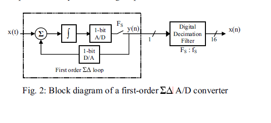
Well the above one is the basic block diagram of a first order sigma delta ADC. Now I am trying to implement that in hardware. Here's the image that I saw regarding the implementation in hardware. I have few doubts here. The integrator that is present in the block diagram above is not present in the circuit below but rather we have a RC integrator at the output of DAC which is not the case above. I tried this circuit and I am getting the Delta modulated signal at the output of the DFF. But my question is this- Will we get the same noise shaping as that of the basic block diagram? I am having a doubt because both circuits seem to be different. Will we get the same maximum possible SNR for both circuits for a given OSR?


Thanks a lot
 

It would be better if you used an external opamp integrator instead of a simple RC.

The RC might work well only if your input signal is very small and centered at Vdd/2. In other case your "integrator" would be a RC charge/discharge curve, not a straight line.
 

Ya that's okay. But you didn't answer my doubts. Eagerly waiting for your reply

Thanks
 

As said, low-pass transfer function is different from integrator, thus you get different noise shaping. You may want to calculate it using the Schreyer's popular Matlab toolbox or a different method of your choice.

First order SD noise shaping isn't mind blowing in any case, also the transfer function is at least similar to an integrator based SDM. I don't expect huge differences.
 

Thanks so much for the reply. But one thing bothers me a lot. That integrator in the SD block diagram is placed after the difference whereas here the RC filter is placed after the DAC output. This should mean a different Transfer function right?

Thanks a lot
 
  • Like
Reactions: FvM

    FvM

    Points: 2
    Helpful Answer Positive Rating
Yes, you are right. I overlooked this important detail. You would need another low-pass at the signal input to get a transfer function nearer to the integrator.
 

Ya but I took that from one IEEE paper. This should mean the above mentioned method also should work. Besides what they have written is that the output of the RC filter tracks the input signal.

Thanks
 

Status
Not open for further replies.

Part and Inventory Search

Welcome to EDABoard.com

Sponsor

Back
Top