Continue to Site

Welcome to EDAboard.com

Welcome to our site! EDAboard.com is an international Electronics Discussion Forum focused on EDA software, circuits, schematics, books, theory, papers, asic, pld, 8051, DSP, Network, RF, Analog Design, PCB, Service Manuals... and a whole lot more! To participate you need to register. Registration is free. Click here to register now.

read stability of 6t sramcell by changing cell ratio

Status
Not open for further replies.

the_pro

Junior Member level 1
Joined
Apr 28, 2012
Messages
15
Helped
0
Reputation
0
Reaction score
0
Trophy points
1,281
Activity points
1,381
hello...every one.
i have used 6t sramcell in my SRAM design.

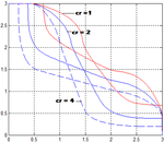
for the read stability , i have optimized my cell by changing the cell ratio (ratio of the width of pull down nmos to pass nmos transistor) from 1 to 4. i kept pull up transistor width fix.

i observed that from cell ratio 1 to 2 , my read SNM improved but from 2 to 4 it again degraded.
and it is clear that if i will go beyond 4 then it will give less read SNM.
i have attached butterfly curve resutls.

is this result right ?
give me your suggestions .... thank u.
Untitled.png
 

Looking only at one metric is not sufficient to optimize the cell. Did you consider other metrics, and variation over PVT corners?
 

hi...

right now, i am doing size modulation.

my work plan is as follows:
1) size modulation
-> cell ratio (pull down to access transistor)
-> pull up ratio (pull up to access transistor)

2) voltage modulation
-> bit line voltage
-> word line voltage
-> data retention voltage

but, i came to know that this all are inter dependent.
like.... if i will change pull up transistor width then my CR can be changed.
so, i confused. there are so many combination of Wp, Wa and Wn.

so how can i proceed further ?
what should be my proper work flow ?

thanks a lot for reply....

It is a real multi-dimensional optimization problem, where a set of spec (write time, power, stability, area, ...) depend on a set of design parameters (cell ratio, bit line voltage, ...). There are additional parameters like temperature and process variation that you cannot influence, but you have to consider during optimization because they have a strong effect on the performance.
Such problems are best solved by numerical circuit optimization software. If you do it manually without such software, then you have only a choice between two bad approaches:
a) equation-based: quite tedious and error-prone to develop, only rough approximations, not good for multi-corner
b) one-by-one: tune one spec after the other by its most sensitive parameter. Works for simple analog circuits that are constructed with this method in mind, but not well for your problem with trade-offs and no simple 1:1 mapping between parameter and spec.
Disclaimer: my company (www.muneda.com) sells circuit optimization software, some use it for bit cell optimization, you can check the website. If you are more scientifically interested in developing the algorithm for yourself, you could also try with Matlab.
 

    V

    Points: 2
    Helpful Answer Positive Rating
thanks a lot sir,

can i have a more information about this software ?
can you provide a direct link to this software manual ?
 

thanks a lot sir,

can i have a more information about this software ?
can you provide a direct link to this software manual ?

Dear the_pro,
there is public information available at the website www.muneda.com ; for more specific internal information (such as algorithmic questions, tutorial, software environment, ...), please contact info@muneda.com .
Best Regards,
Michael
 

Status
Not open for further replies.

Part and Inventory Search

Welcome to EDABoard.com

Sponsor

Back
Top