Continue to Site

Welcome to EDAboard.com

Welcome to our site! EDAboard.com is an international Electronics Discussion Forum focused on EDA software, circuits, schematics, books, theory, papers, asic, pld, 8051, DSP, Network, RF, Analog Design, PCB, Service Manuals... and a whole lot more! To participate you need to register. Registration is free. Click here to register now.

ICMR of an NMOS input Op-Amp

Status
Not open for further replies.

Junus2012

Advanced Member level 5
Joined
Jan 9, 2012
Messages
1,552
Helped
47
Reputation
98
Reaction score
53
Trophy points
1,328
Location
Italy
Activity points
15,235
Hello Analog heroes

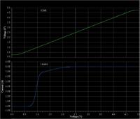
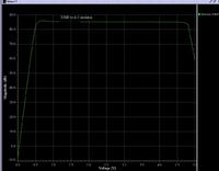
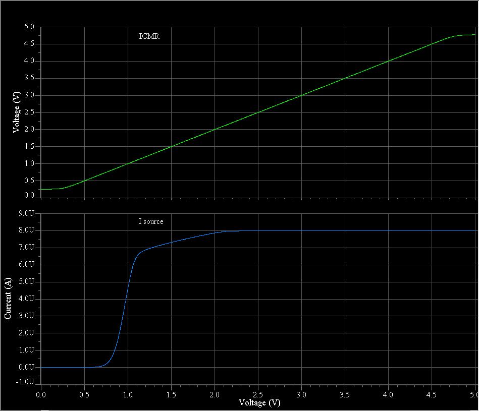
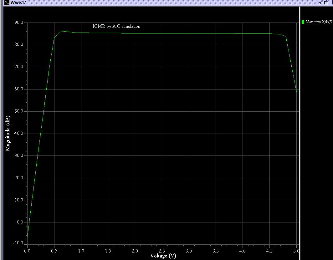
I finished design of an NMOS input OTA, I used a cascode current source and I was expecting to get bad low ICMR, but I surprised with the result. as you can see the cascod current source start to saturate at 2.3V while the ICMR start showing linear behavioural at 0.25V. then I did the ICMR test by sweeping the VCM from the A.C analyses as shown in the second image, the result always the same

What are the reason behind that?


Thank you very much
 

I would ask another related question

is there any reliable method to simulate the ICMR rather than the methods I used ??
 

What are the reason behind that?

I guess you used different values for the independent (horizontal) axes: DC input resp. output voltage for the ICMR simulations, operation voltage for the current source sim? Always describe what your axes present!
 

hello erikl
in the first graph, the circuit is connected as a unity gain buffer, then I sweepd the input voltage (Vin+ = VIC) in the D.C analyse which represent the X-axes, Vo represent the output voltage in the y-axses. in the same graph 1 the second plot represent the corresponded current behavioural of the current source of the Op-Amp with respect to the VIC.

the second graph represent the simulation of the ICMR using a.c simulation, here in the x-axis is the VIC and y-axses represent the maximum gain.

I hope it is clear now for you,
and thank you very much for your reply
 

I hope it is clear now for you
No, sorry it is not yet clear, because you didn't tell where you measured the "current behavioural of the current source" and what is Vin- voltage during the simulation.

For such questions, better post the corresponding schematic showing all your stimulation and measurement points.
 

dear erikl
the simulation of the current source in the D.C analyses (first graph) is done simultaneously with the change of VIC (in the x-axsis), it is simply by monitoring the drain current of the current source transistor which is cascod current source mirror. you can see the point at which the current start to saturate

I am sorry if is still not clear,
thanks alot
 

Hi senan,

Simulate OPAMP with buffer feedback configuration. And then run Vin from 0v to Vdd:

ICMR.JPG
The simulation result will be looked like this:
ICMR2.JPG

Have fun!
 
Dear ducvilla

i did exactly what you suggested before and I got the graphs (the first image ) that is similar to yours. the confection point is why we would show the output while we still need to refer to the current source status as you can see from your graph
the second thing is how we are assuring that the output voltage is only affected by the input common mode voltage why not from the output limitation.

can you please tell me from which source you got this graph and the page Nr. if possible ?
thank you very much
 

Hi Senan,

I got the simulation result based on the book:"Analysis and Design of Analog Integrated Circuit" 4th Edition. Also, as you see the definition of ICMR, it seems does not relate to Vout, just only Vin (if that, you do not need to plot Vout in graph). But ICMR is affected by output swing (as you mentioned in the 2nd question of your previous post), so that you should consider it in simulation result.

In detail, i take an example of typical basic two stages OPAMP like:
Basic two stages OPAMP type P:

basic two stages opamp type P.JPG

Vt3 - |Vt1| + |Vov3| <= Vic <= Vdd - |Vt1| - |Vov1| - |Vov5|

And for basic two stages OPAMP type N:

basic two stages opamp type N.JPG

Vt1 + Vov1 + Vov5 <= Vic <= Vdd - Vt1 - |Vt3| - |Vov3|

Actually, another thing view from this point is if your design requires larger output swing, you should choose OPAMP type P.

Hope this help!
 
Dear ducvilla
thank you again for your participation
Just want to notify that when you want to simulate the ICMR, there should be no effect from the output. any way if you cconsider your second equation for the NMOS input stage Op-Amp you will see it is above the ground by the value of (Vt1 + Vov1 + Vov5 ), and suppose now if you have replaced t he simple current source with cascod one as in the case of my design, then you will get a worse value...... However if you look to the graph that I showed in the first image, it seem to be that min ICMR is not affected by the cascod connection unless if you take in the account the current source graph as you showed in the first reply of you.

BUT ALSO

go back to the ICMR graph, why the author considered the start of the ICMR range from the moment of the current source (M5) entered the saturation region, it mean he ignored the input transistors saturation condition (Vt1 + Vov1 )???????

Please if you can give me the page Nr. of the ICMR graph

Thank you all once again
 

Status
Not open for further replies.

Part and Inventory Search

Welcome to EDABoard.com

Sponsor

Back
Top