Continue to Site

Welcome to EDAboard.com

Welcome to our site! EDAboard.com is an international Electronics Discussion Forum focused on EDA software, circuits, schematics, books, theory, papers, asic, pld, 8051, DSP, Network, RF, Analog Design, PCB, Service Manuals... and a whole lot more! To participate you need to register. Registration is free. Click here to register now.

How to read ADC0804 into 89S52

Status
Not open for further replies.
Joined
Apr 8, 2012
Messages
201
Helped
3
Reputation
6
Reaction score
2
Trophy points
1,298
Activity points
0
Hello!
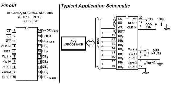
Can somebody check the attached file and explain me how to get the adc value into uP?

I want to know the exact steps for reading ADC 0804 into 89S52.

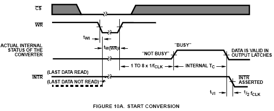
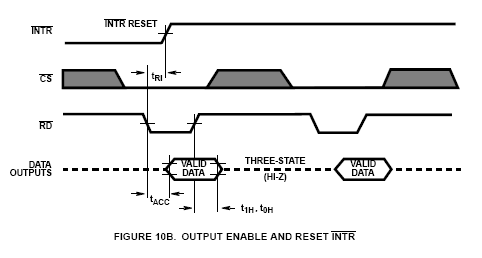
Please mention step by step the reading process, like which pins of ADC 0804 have to be set high / low for enabling the ADC to read the analog input and how to make the ADC to place the o/p on its o/p port. how to read the o/p of ADC from 89S52.
 

Attachments

  • ATMEL89C52.rar
    20.1 KB · Views: 110
Last edited:

I want to know how to make the adc 0804 read analog signals and then place the o/p on its o/p port [D0-D7]/
 

ok see basically adc0804 has only one input channel.


adc0804.gif


You need a minimum of 11 pins to interface ADC0804, eight for data pins and 3 for control pins. As shown in the typical circuit the chip select pin can be made low if you are not using the microcontroller port for any other peripheral (multiplexing).


adc0804-timing.gif


The above timing diagrams are from ADC0804 datasheet. The first diagram shows how to start a conversion. Also you can see which signals are to be asserted and at what time to start a conversion. So looking into the timing diagram . We note down the steps or say the order in which signals are to be asserted to start a conversion of ADC. As we have decided to make Chip select pin as low so we need not to bother about the CS signal in the timing diagram. Below steps are for starting an ADC conversion. I am also including CS signal to give you a clear picture. While programming we will not use this signal.

Make chip select (CS) signal low.
Make write (WR) signal low.
Make chip select (CS) high.
Wait for INTR pin to go low (means conversion ends).


Once the conversion in ADC is done, the data is available in the output latch of the ADC. Looking at the FIGURE 10B which shows the timing diagram of how to read the converted value from the output latch of the ADC. Data of the new conversion is only avalable for reading after ADC0804 made INTR pin low or say when the conversion is over. Below are the stepts to read output from the ADC0804.

Make chip select (CS) pin low.
Make read (RD) signal low.
Read the data from port where ADC is connected.
Make read (RD) signal high.
Make chip select (CS) high.


adc0804-timing1.gif


---------- Post added at 08:56 ---------- Previous post was at 08:55 ----------

hope it helped !!!
 
  • Like
Reactions: ximki

    ximki

    Points: 2
    Helpful Answer Positive Rating
I tried your method, but I can't get the right value. It is giving some 13.9999. Please check my Project attached with this post.

Can you give me the C code for the adc part?
 

Attachments

  • prj.rar
    21.6 KB · Views: 104

Check this also...
 

Attachments

  • prj2.rar
    21.7 KB · Views: 110

sorry i was a bit busy with some work , will see your project and reply soon
 
  • Like
Reactions: ximki

    ximki

    Points: 2
    Helpful Answer Positive Rating
sorry i was a bit busy with some work , will see your project and reply soon
Hi ^_^, can you post here the assembly code how you read data from ADC0804 and show them in 7Seg Display
 

Status
Not open for further replies.

Similar threads

Part and Inventory Search

Welcome to EDABoard.com

Sponsor

Back
Top