Hand assembly and soldering of individual pin arrays to a PCB is inefficient, costly, and results in poor product quality. Yet, some manufacturers are still doing this.
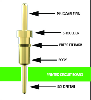
One old-school production soldering method employed for thru-hole PCB assemblies is called wave-soldering. To accomplish wave soldering, a pin solder tail is inserted through a PCB plated thru-hole. There are several critical dimensional relationships between the pin solder tail and PCB.
This article will focus on solder tail features required for wave soldering processes. We will review the following:
1. General comments and considerations
regarding solder tail termination.
2. PCB assembly considerations when using as a
single, standalone pin.
3. Advantages of packaging pins into molded
insulators
You will need to weigh the pros and cons of each, selecting the easiest process to implement producing cost-effective results.
I. General comments/ Design considerations:
Wave soldering is one of the most common, easiest to perform, time-proven methods of attaching solder tail pins to a PCB.
Tail length: The solder tail should protrude at least 0,25mm below the PCB for solder fillet formation.
If the pin lead does not protrude beneath the PCB during wave soldering, wicking will be adversely affected.
If the pin lead is protruding greater than 2,54mm, it may act rudder-like in the soldering process and create troublesome bridging.
Tail diameter: To promote solder wicking, the plated hole should provide a minimum of 0,05mm clearance to the m pin lead. If there is no clearance but rather an interference fit, then wicking will not occur. Solder wicking may also be affected by thick PCBs with internal planes acting as heat-sinks.
II. Single Position Solder Tail Pin Applications:
Vertical instability: A single solder tail placed into a PTH will most likely tilt depending on the amount of clearance between the hole and tail diameter. They must never be the same diameter as no tail-to-hole clearance will prevent solder wicking.
If you require a single pin in your application, look for one with a flat bae feature for vertical alignment and stability.
Tail length: The solder tail should protrude at least .010 below the PCB to create a solder fillet.
III. Packaging Solder Tail Pins in Insulators:
Packaging the pin into a molded or machined insulator provides not only vertical stability but also mechanical strength. An insulator body may also provide a surface for automated pick and place.
Summary:
If pin density is not critical in your application, and you do not intend to assemble components on both sides of your PCB then through-hole solder tail interconnects will provide superior mechanical strength and pattern alignment.
Comments and suggestions are always welcome.
PDF:

 drive.google.com


One old-school production soldering method employed for thru-hole PCB assemblies is called wave-soldering. To accomplish wave soldering, a pin solder tail is inserted through a PCB plated thru-hole. There are several critical dimensional relationships between the pin solder tail and PCB.
This article will focus on solder tail features required for wave soldering processes. We will review the following:
1. General comments and considerations
regarding solder tail termination.
2. PCB assembly considerations when using as a
single, standalone pin.
3. Advantages of packaging pins into molded
insulators
You will need to weigh the pros and cons of each, selecting the easiest process to implement producing cost-effective results.
I. General comments/ Design considerations:
Wave soldering is one of the most common, easiest to perform, time-proven methods of attaching solder tail pins to a PCB.
Tail length: The solder tail should protrude at least 0,25mm below the PCB for solder fillet formation.
If the pin lead does not protrude beneath the PCB during wave soldering, wicking will be adversely affected.
If the pin lead is protruding greater than 2,54mm, it may act rudder-like in the soldering process and create troublesome bridging.
Tail diameter: To promote solder wicking, the plated hole should provide a minimum of 0,05mm clearance to the m pin lead. If there is no clearance but rather an interference fit, then wicking will not occur. Solder wicking may also be affected by thick PCBs with internal planes acting as heat-sinks.
II. Single Position Solder Tail Pin Applications:
Vertical instability: A single solder tail placed into a PTH will most likely tilt depending on the amount of clearance between the hole and tail diameter. They must never be the same diameter as no tail-to-hole clearance will prevent solder wicking.
If you require a single pin in your application, look for one with a flat bae feature for vertical alignment and stability.
Tail length: The solder tail should protrude at least .010 below the PCB to create a solder fillet.
III. Packaging Solder Tail Pins in Insulators:
Packaging the pin into a molded or machined insulator provides not only vertical stability but also mechanical strength. An insulator body may also provide a surface for automated pick and place.
Summary:
If pin density is not critical in your application, and you do not intend to assemble components on both sides of your PCB then through-hole solder tail interconnects will provide superior mechanical strength and pattern alignment.
Comments and suggestions are always welcome.
PDF:
CT003.pdf
 drive.google.com
