sprinto
Newbie level 3
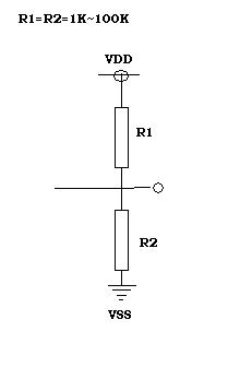
high impedance value
Suppose V(high)=1.5v for logic 1 and V(low)=0v for logic 0 . Generally what should be the voltage value of Z-HIGH IMPEDANCE state?.
To elaborate,
In bi-directional IO operations we usually make use of this Z state(using GZ pin) . Z state is used to transmit no LOGIC. But how is this done?. Is it completely disabling/disconnecting the port or making it to reach a voltage value which does not imply any logic.
") ..
..