Continue to Site

Welcome to EDAboard.com

Welcome to our site! EDAboard.com is an international Electronics Discussion Forum focused on EDA software, circuits, schematics, books, theory, papers, asic, pld, 8051, DSP, Network, RF, Analog Design, PCB, Service Manuals... and a whole lot more! To participate you need to register. Registration is free. Click here to register now.

XC6SLX9 XCF04 design

Status
Not open for further replies.

asadi.siyavash

Member level 4
Joined
Feb 14, 2013
Messages
68
Helped
2
Reputation
4
Reaction score
2
Trophy points
1,288
Activity points
1,769
Hi,
I'm new with xilinx FPGA before this project I designed Altera FPGA's like cyclone II and III without any problem. but now my Spartan 6 design doesn't work. I attached my schematic. when I scan JTAG it said no hardware connected.
I have these questions:
1.is the connection of JTAG right? I draw it like "Spartan-6 FPGA Configuration Guide"
2.my oscillator doesn't work very well! it has 1volt offset and also it peak to peak voltage is 1 volt?
3.all of FPGA PIN are high! I changed my FPGA but it was high too.
I am really confused please help me it is urgent.
excuse me for my bad english.
 

Attachments

  • FPGA_SPARTAN6.PDF
    620.1 KB · Views: 68

Your oscillator should have pin-1 unconnected E/D should be unconnected to enable the oscillator. As an example look at this vectron part https://www.vectron.com/products/xo/VC-820.pdf

If your JTAG connector P4 is numbered with 1-7 on one side and 8-14 on the other side, then it's probably not connected correctly unless you made your own board layout for the connector. Connectors are normally numbered with even numbers on one side and odd numbers on the other. See page 14 of the following Xilinx document: https://www.xilinx.com/support/documentation/data_sheets/ds593.pdf

You will have to resort to hooking the JTAG pod up with the flying leads. Make sure you connect TDI of the leads to J_TDI of your connector and TDO of the leads to J_TDO of the connector

You also shorted DONE to gnd if you have R48 installed.

Don't notice anything else right now.

Regards
 

Hi really thanks for spending time for replying to me,
If the Oscillator don't work Xilinx ISE don't recognize hardware?
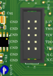
I designed Jtag Connector like what said in "Spartan-6 FPGA Configuration Guide" I attached my PCB of JTAG connector. it is exactly same with page 14 of the Xilinx document that you recommended.
and about R48 yes I don't installed it now. I just connect 330Ohm (R45) and pull up Done PIN to 3.3V. but one thing here is strange when I read the voltage of DONE pin it was 0.1 Volt ! is it normal?
I'm really confused I design as like as Documents of Spartan 6.
JTAG.PNG
 

The oscillator won't stop the FPGA from configuring. You just mentioned one of the problems you were seeing.

Why is there a 10-pin connector installed on your PCB? The standard Xilinx connector to the USB pod is a 14-pin connector with the following standard layout.
Capture1.PNG

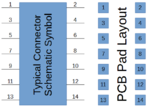
The silkscreen on the PCB isn't the same as the electrical connectivity of the pins on the connector. Is the PCB layout of your schematic symbol like Layout A or Layout B?
Capture2.PNG

If you made a custom PCB layout for you schematic symbol like Layout B then it should match the Xilinx JTAG pod connector. If you made a custom symbol but used a standard PCB layout from a library then you probably have Layout A on the PCB, which would result in the connections not matching the Xilinx JTAG pod connector. In this case the following connections would be on the PCB.

Code:
pin1     Gnd    Gnd     pin2
         Gnd    Gnd
         Gnd    Gnd
         Gnd    VCCAUX
       J_TMS    J_TCK
       J_TDO    J_TDI
pin13     NC    NC      pin14
Verify the connections on the PCB between the connector, FPGA, and platform flash to make sure the connections are not like above. If they are then you'll have to either make an adapter cable or use the flying lead set from the Xilinx JTAG pod.

Regards
 

Hi, thanks again,
I use 10 PIN because my connector is 10 Pin.
no it is one of standard symbol library for Altium designer. it is like LAYOUT B.
I am sure all of connections are true, I checked them very carefully.
Is other part of my schematic true?
 

Well if you connector is 10 pin then you aren't using a Xilinx JTAG programming pod. Did you make sure the pinout of your pod matches the connector pinout on the PCB?

You say the connections are true and you checked them carefully. Did you check them on the PCB with an ohm meter?

JTAG supersedes all other programming modes, so it shouldn't matter how you connect the rest of the circuit outside of correctly connecting power and ground to the FPGA and making sure that the dedicated programming pins aren't shorted/force to the wrong state after power is applied.

As your original post stated.
when I scan JTAG it said no hardware connected.
That means you must have the wrong connections to the JTAG programming pod (with the 10-pin connector) that you are using. Make sure that the programming pod you are using considers TDO an INPUT to the pod and that TDI is the output.
Given that you chained FPGA-TDO to Flash-TDI:
POD-TDO <== Flash-TDO
POD-TDI ==> FPGA-TDI
for a Xilinx or Xilinx like pod

If the pod uses the opposite nomenclature: Pod thinks TDO is it's output and TDI is it's input.
POD-TDO ==> FPGA-TDI
POD-TDI <== Flash-TDO

- - - Updated - - -

Have you tried putting a scope on TCK on the FPGA and see if there is a clock when you try to connect to the target? There should be a number of TCK clocks generated by the pod when it analyzes the chain.

- - - Updated - - -

Oh, I forgot to mention previously that the DONE pin being driven low after power up is normal. It won't go high until the FPGA is configured.
 

Status
Not open for further replies.

Part and Inventory Search

Welcome to EDABoard.com

Sponsor

Back
Top