Continue to Site

Welcome to EDAboard.com

Welcome to our site! EDAboard.com is an international Electronics Discussion Forum focused on EDA software, circuits, schematics, books, theory, papers, asic, pld, 8051, DSP, Network, RF, Analog Design, PCB, Service Manuals... and a whole lot more! To participate you need to register. Registration is free. Click here to register now.

Why voltage drops between drain and source of Mosfet

Status
Not open for further replies.

nihan_A

Newbie level 5
Joined
Apr 11, 2018
Messages
8
Helped
1
Reputation
2
Reaction score
0
Trophy points
1
Activity points
131
Hello!

I have a problem with driving P channel mosfet.
I am trying to control power voltage of a TFT. As you can see below when TFT_Power_EN signal is low I expect there would be 3.3V at the Drain of the mosfet which is labeled as TFT Power. But when I check the signal it is just 2.5V
I understand, since mosfet has its own resistance there would be some loss. But when I check mosfet datasheet 0.8V loss is too much.
I thought maybe TFT wants to draw more current so it result voltage drop so I connect one more mosfet as parallel but no change.
If anyone have experience or any idea please help me.
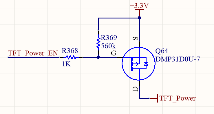
1600786469434.png


P.s. Measured current from the drain is 460ma with 2.5V drain voltage
 

Considering transistor heating, the voltage drop is still in the expectable range. You need a transistor with lower Rds,on and higher current rating for this application.
 

Sim and part specs look OK.

1600789878284.png


What is your gate drive level ? This is the backlight of the TFT, right ? Which I used a
6 ohm as drain load, but should be a diode drop of LEDs in backlight ? Or does this
supply a DC/DC in TFT that in turn drives B/L ?

If Vgs is - 3.3 the typical curves show ~ .5 ohms Rdson, which should be OK. But you
should look at worst case. Worst case at Vgs of -2.5 is ~ 1.5 ohms


Regards, Dana.
 
Last edited:

Your simulation doesn't reflect junction overtemperature due to power dissipation.
 

Power in device quite low, roughly ~ 100 mW, not really a consideration. Top curve.

1600792382723.png
.

Regards, Dana.
 

The sim shows Vds << .8 V, thats why the power curve shows the ~ 100 mW.

To your point sim is only run at 25 C.

The Id vs T shows a less than doubling 25C to 150C, ambient.

1600794017870.png


But above curves typ and at Vgs -4.5.

If I look at a "typ" Rdson vs T -

1600794774120.png


We see it is impacting circuit Pdiss via rise in it.

I would have to use a different sim to get at the DC situation in a more complete fashion,
non withstanding accuracy of spice model issues.


Regards, Dana.
 
Last edited:

Always read the data sheet carefuly for worst case Vgs, Rds-on and power dissipation for minimum footprint .....!
 
  • Like
Reactions: FvM

Hi,

...when TFT_Power_EN signal is low I expect there would be 3.3V at the Drain of the mosfet which is labeled as TFT Power. But when I check the signal it is just 2.5V

Stupid question, sorry to ask:

What do you mean in volts when you say "...when TFT_Power_EN signal is low..."? When it's at 0V and turning the PMOS on?
 

Thank you all for replying.

Sim and part specs look OK.
What is your gate drive level ? This is the backlight of the TFT, right ? Which I used a
6 ohm as drain load, but should be a diode drop of LEDs in backlight ? Or does this
supply a DC/DC in TFT that in turn drives B/L ?

If Vgs is - 3.3 the typical curves show ~ .5 ohms Rdson, which should be OK. But you
should look at worst case. Worst case at Vgs of -2.5 is ~ 1.5 ohms

Regards, Dana.

Yes it is just DC supply. My gate drive level is 0V for case mosfet on and 3.3V for off.

Considering transistor heating, the voltage drop is still in the expectable range. You need a transistor with lower Rds,on and higher current rating for this application.

I want to inform you all Mosfet is not really heating much while TFT draws 460mA. It is lower than 40 C. And I tried to divide current by adding one more mosfet as parallel but it made no change.

Hi,

Stupid question, sorry to ask:

What do you mean in volts when you say "...when TFT_Power_EN signal is low..."? When it's at 0V and turning the PMOS on?

Yes, it is 0V so mosfet should turn on.
 

    d123

    Points: 2
    Helpful Answer Positive Rating
I want to inform you all Mosfet is not really heating much while TFT draws 460mA. It is lower than 40 C.
If your voltage and current measurements are real, the calculated power and delta T numbers are correct as well. The value is for junction temperature, case temperature may be considerably lower.

An optimistic assumption would be that the transistor voltage drop and power dissipation are actually lower and the voltage is dropped somewhere else...
 
You can't parallel MOSFETS without using ballasting or active current
circuitry. The variation from one MOSFET to another can produce one part
taking most of the current, the others paralleled not so much.


Regards, Dana.
 

Hi,

I agree that paralleling BJTs is problematic without balancing.
But paralleling MOSFETs is not that problematic. For sure the wiring/PCB layout should care for about identical source serial resistances.

Klaus
 
In this part the Vth variance device to device is > 2:1.

In linear region
1600899592440.png


In sat region
1600899642669.png


Only if Vgs >> Vth is Vth variance of lesser concern. In case of logic level MOSFETs
Usable Vgs range in most designs leave Vth with significant effect.

There is a very strong dependence on basic device parameters of Idrain, so I
register disagreement on paralleling unless precautions are taken.


Regards, Dana.
 

Status
Not open for further replies.

Similar threads

Part and Inventory Search

Welcome to EDABoard.com

Sponsor

Back
Top