Continue to Site

Welcome to EDAboard.com

Welcome to our site! EDAboard.com is an international Electronics Discussion Forum focused on EDA software, circuits, schematics, books, theory, papers, asic, pld, 8051, DSP, Network, RF, Analog Design, PCB, Service Manuals... and a whole lot more! To participate you need to register. Registration is free. Click here to register now.

Why use a BJT in an op-amp assisted current source?

Status
Not open for further replies.

sjb741

Junior Member level 2
Joined
Aug 6, 2021
Messages
20
Helped
0
Reputation
0
Reaction score
1
Trophy points
3
Activity points
222
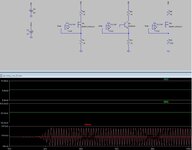
In AoE - The x-chapters, fig 4x.124 shows a way to cancel the error due to non-zero base current. The circuit sinks 100mA.

When would a designer choose a BJT over a MOSFET in this circuit, given the MOSFET has such a small gate current requirement - for better frequency response?

<EDIT> I simulated this and to my surprise the MOSFET version oscillated but the BJT variant behaved.
At 10mA though, the MOSFET version is fine.

I think the MOSFET used is not too crazy, I tried to chose a 'not too large' gate charge and fairly small Rds.
 

Attachments

  • op-amp_I_src_01.zip
    1.1 KB · Views: 98
  • op-amp_I_src_01.jpg
    op-amp_I_src_01.jpg
    139.8 KB · Views: 149
Last edited:

Using a high current FET with 5 nF Cgs is is a way off. No surprize that the circuit is oscillating. Use a FET comparable with the low current BJT or use suitable compensation means.
 

From the datasheet -

1651509756699.png


As FvM mentioned, the Zout of the OpAmp coupled with large Cload
creates phase shift, in this case apparently enough to create the
phase shift to produce + fdbk, hence oscillations.


Regards, Dana.
 

When would a designer choose a BJT over a MOSFET in this circuit, given the MOSFET has such a small gate current requirement - for better frequency response?

MOSFETs are not necessarily faster since you have to drive their large gate capacitance.
In a sort of emitter-follower mode, as used here, the BJT is likely as fast or faster than a MOSFET.

The main advantage of a MOSFET is that it has no gate current to cause an error (difference) in the drain current versus the source current.
 
One primary reason is that these app notes are ancient and
the BJT was around and in use before the op amps.

Another is that MOSFETs (small gate area ones, anyway) are
noisy relative to good quality BJTs.

A small signal MOSFET like ALD makes, is a whole 'nother
critter from the power MOSFET most people think of.

You can steer BJT current with a whole lot less base voltage
excursion, than you can a MOSFET. That soaks up less BW /
stability margin, as a follower. Power MOSFET with a high VT
(many are 4-6V looking for 10V gate drive) will lose you a lot
of headroom; a small logic-level FET might do better.

Some LDMOS, VDMOS FETs are good for "on, or off, make
your mind up as quickly as possible but not so quickly that
drain dV/dt gets you..." but have "a lot of corner cut off the
SOA". I've burned up integrated small LDMOS by taking too
long on the curve-pull.
 
Thanks for the replies!

Whilst I was aware that gate capacitance could be a problem for the op-amp, I simply searched the LTSpice list for 'fairly low gate charge in comparison with the others in the list'. I should have checked more carefully, especially in relation to the chosen op-amp's output charcteristics.

Good point about the size of signal excursion required to drive a 'gate' in comparison with a 'base'.

I've used MOSFETs successfully in the past for about 20mA, for example BSS138+MCP6005 or TN0200K+TLV2624. This perhaps made me too confident.

I'd like to be able to model this such that I see where & how the problems arise. Maybe an ideal op amp plus some parts to model the LT1797 output characteristics, then some capacitance(s) to model the gate charge. Then use an ideal buffer to drive the BJT, and see what it takes to spoil the BJT's good performance.

I am especially curious about the way the MOSFET used in the simulation seems fine at lower currents - this might tie in to the point about size of signal excursion?

A complicating factor is that gate capacitance varies with gate drive - the capacitances are voltage dependent I seem to recall.
 

It's generally possible to design OP controlled MOSFET current sources for all current levels and different bandwidth requirements. This possibly involves low impedance analog gate drivers and well considered frequency compensation. If required control bandwidth is low, a standard OP can still work.
 

Hi,

I guess all my designed 4..20mA industrial current sources/sinks are made with MOSFETs.

Klaus
 

Thanks for the replies!

Whilst I was aware that gate capacitance could be a problem for the op-amp, I simply searched the LTSpice list for 'fairly low gate charge in comparison with the others in the list'. I should have checked more carefully, especially in relation to the chosen op-amp's output charcteristics.

Good point about the size of signal excursion required to drive a 'gate' in comparison with a 'base'.

I've used MOSFETs successfully in the past for about 20mA, for example BSS138+MCP6005 or TN0200K+TLV2624. This perhaps made me too confident.

I'd like to be able to model this such that I see where & how the problems arise. Maybe an ideal op amp plus some parts to model the LT1797 output characteristics, then some capacitance(s) to model the gate charge. Then use an ideal buffer to drive the BJT, and see what it takes to spoil the BJT's good performance.

I am especially curious about the way the MOSFET used in the simulation seems fine at lower currents - this might tie in to the point about size of signal excursion?

A complicating factor is that gate capacitance varies with gate drive - the capacitances are voltage dependent I seem to recall.

Thats correct on C = f(V) -


Regards, Dana.
 

Status
Not open for further replies.

Similar threads

Part and Inventory Search

Welcome to EDABoard.com

Sponsor

Back
Top