mpig09
Full Member level 4
Hi all:
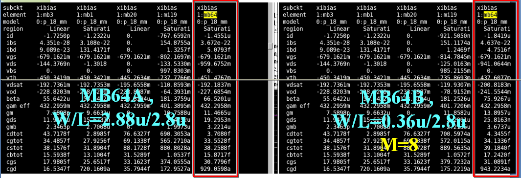
I design a PMOS current mirror, and the current ratio is 1:2:4:8.
There are two kinds of width ratio to get 1:2:4:8. (the same L=2.8u, Process is 0.153um)
1st : MB61A, W=0.36u 2nd: MB61B, W=0.36u, m=1
MB62A, W=0.72u MB2B, W=0.36u, m=2
MB63A, W=1.44u MB63B, W=0.36u, m=4
MB64A , W=2.88u MB64B, W=0.36u, m=8
The simulation shows the IMxA < IMxB (ex: IMB64A < IMB64B)
and Vth, MxA > Vth, MxB.
Please the attached file for hspice .lis.
My question are :
1. why Vth, MxA > Vth, MxB?
ex : Vth, M64A > Vth, M64B.
2. Why IMxA < IMxB
ex: IMB64A < IMB64B
Thanks.
mpig