alexyangfox
Newbie level 6
- Joined
- Dec 2, 2010
- Messages
- 12
- Helped
- 1
- Reputation
- 2
- Reaction score
- 1
- Trophy points
- 1,283
- Location
- Chengdu,sichuan,China
- Activity points
- 1,417
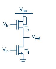
The book says ,
the DC output level is not well-defined.
When the DC voltages of Vb,Vin and Vdd are defined,
I think if I have the equations for Id of the two MOSFETS equal,
I can have a solution for Vout.
If so, Vout shouldn't be not well-defined.
could anyone explain this to me?
Thank you in advance.
yours sincerly ,
alex.