Simranjeet Singh
Junior Member level 3
- Joined
- Feb 10, 2012
- Messages
- 31
- Helped
- 13
- Reputation
- 26
- Reaction score
- 13
- Trophy points
- 1,288
- Location
- Noida, India, India
- Activity points
- 1,465
LVS: Check wikipedia page. Its given very clearly over there.
https://en.wikipedia.org/wiki/Layout_Versus_Schematic
Timing Closure: By timing closure it means that all the timing criteria like setup and hold constraints are satisfied and the design works fine at the specified frequency thats all.
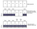
Filler Cells are nothing special...they are just empty cells used to fill the design to maintain a uniform density and for power and ground rail continuity.
The Diagram will explain the use of filler cells for Power continuity.**broken link removed**
Mask: It is simply an arrangement of opaque and transparent areas that is used to create a pattern.
Substrate, nwell, N+, P+ are all part of base layer..
