Continue to Site

Welcome to EDAboard.com

Welcome to our site! EDAboard.com is an international Electronics Discussion Forum focused on EDA software, circuits, schematics, books, theory, papers, asic, pld, 8051, DSP, Network, RF, Analog Design, PCB, Service Manuals... and a whole lot more! To participate you need to register. Registration is free. Click here to register now.

why dont connect B S in local area?

Status
Not open for further replies.

xuel

Advanced Member level 4
Joined
Nov 16, 2004
Messages
101
Helped
16
Reputation
32
Reaction score
10
Trophy points
1,298
Activity points
569
24_1166425995.JPG


Why the layout on right side has better noise rejection?

And are there any other advantages or disadvantages?
 

It's very strange. The layout in the right is avioded in most time. It should have worse noise performance. where does the conclusion come from?
 

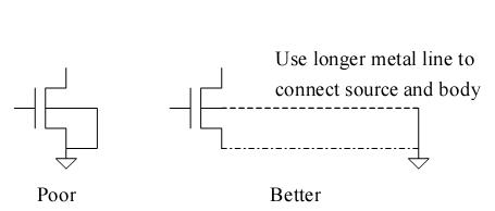
I may have better noise reject as the metal length increases so will the resistance. I have never saw layout done like that, It would create antenna errors and use up vast amount of space not to mention the difficulty in matching devices and routing.
 

renwl said:
It's very strange. The layout in the right is avioded in most time. It should have worse noise performance. where does the conclusion come from?

It's from tsmc layout design rule. I have seen it in both 90nm and 65nm process.
 

I have never seen it in the 0.18um or above process. maybe it's specific to 90nm or less process. can you upload some pages on it?
 

Yes, I see this in the TSMC 90nm design manual.
I'd to know why, too. Can anybody help?
Thanks in advance.
 

any explainations from process manual? i should explain a bit.
 

Status
Not open for further replies.

Part and Inventory Search

Welcome to EDABoard.com

Sponsor

Back
Top