Continue to Site

Welcome to EDAboard.com

Welcome to our site! EDAboard.com is an international Electronics Discussion Forum focused on EDA software, circuits, schematics, books, theory, papers, asic, pld, 8051, DSP, Network, RF, Analog Design, PCB, Service Manuals... and a whole lot more! To participate you need to register. Registration is free. Click here to register now.

Why does gain change with different signal input?

Status
Not open for further replies.

ray.deng

Newbie level 6
Joined
Dec 14, 2009
Messages
12
Helped
0
Reputation
0
Reaction score
0
Trophy points
1,281
Activity points
1,406
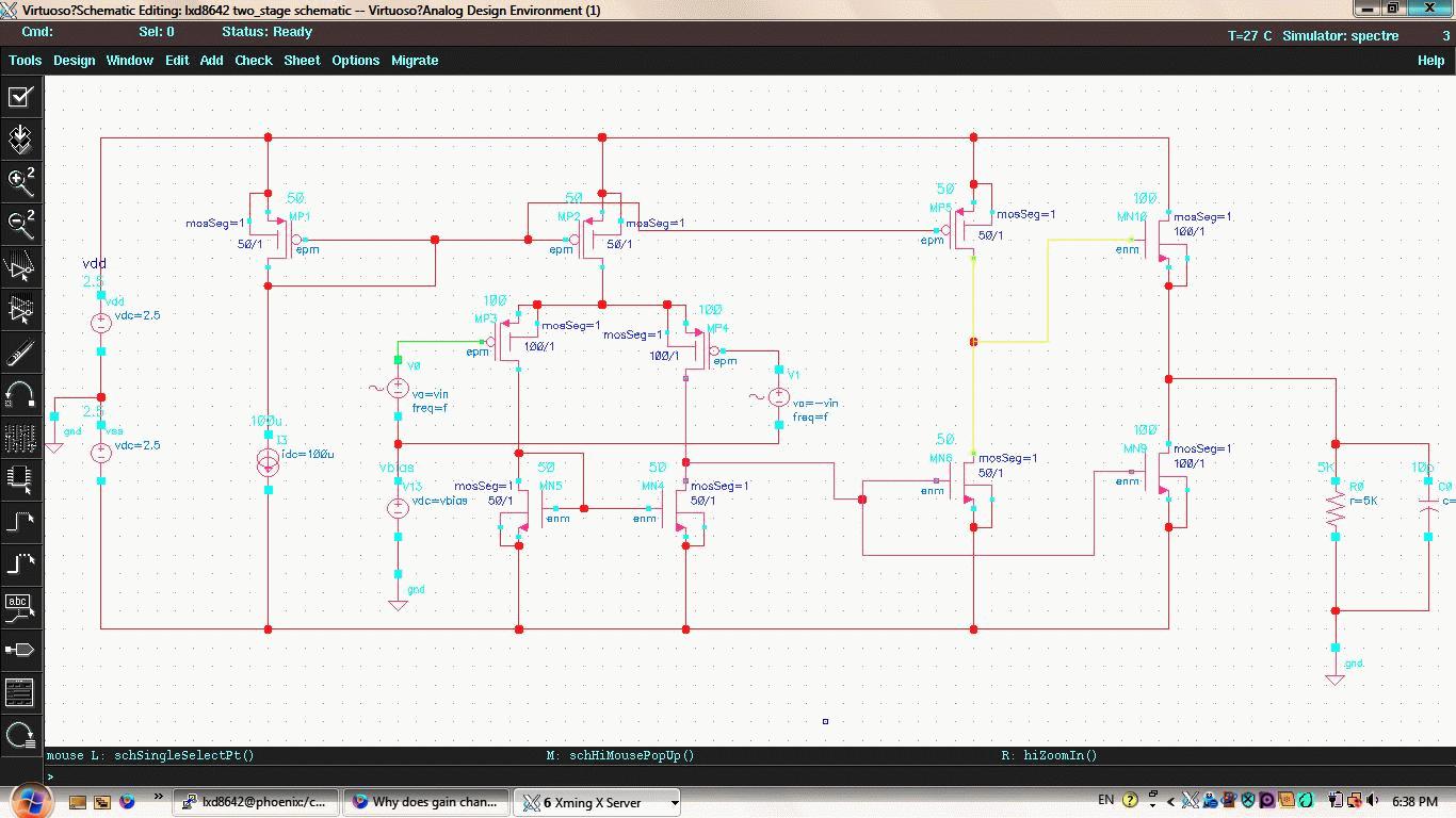
Hi, I was just trying to find the gain of a differential stage using cadence. It's a two stage op amp, with the first stage of single-ended differential and second stage of common source. While I fix the other parameters and configuration and change the signal voltage input of the differential stage from 10mV to 1mV, the gain is changed from about 40 to 80. Can somebody tell me why? Thanks!
 

Maybe you are using an extremely old opamp that has very poor high frequency response (a 741 opamp, an LM358 dual opamp or an LM324 quad opamp) at a frequency that is too high for it.

There are many Sim programs around. Every teacher has their very old favourite. I have never seen Cadence.

Since you didn't post your schematic and parts list then we don't know what you are talking about.
 

how did you measure the gain, run AC or TRAN analysis?
 

Hello ray.deng,

For me,according to your (insufficient) description i suspect a wrong setup of the testbench to measure the low frequency gain of your opamp.You must provide more details,for example what is 40 and 80 you mentioned,dB or clear numbers?Which is the frequency of the 10mV or 1mV signal you insert in the opamp?And how do you check the value of the gain?If possible give a screenshot of your input biasing conditions and signal injection.Without all these information nobody can help you!

Regards,
Jimito13
 

Maybe 10mV is enough to more than steer the front end
and you are compressing. 80dB gain (10000) means 10mV
would become 100V and you are not (I expect) designing
an op amp with that kind of supply or output swing.
 

Hi guys, thanks for the reply. I really appreciate it! Yes, I think I need to use 10uv for signal input instead of 10m and it comes to be OK after I change that. Sorry for not explaining things clearly, for I'm still pretty new to this domain.

---------- Post added at 23:00 ---------- Previous post was at 22:59 ----------

I'm having some other issues here. How do you adjust Vds? Like in the second stage, common source stage, if I want to decrease the drain voltage, what should I do? When I did the simulation, that drain voltage is too high, making the transistor in the output stage in triode region.

I'm using a 0.5um technology, and select the channel length in the schematic to be 1um. How should I choose the typical value for the width?

In the first differential stage, it seems when I change the biasing voltage, the Vdsat of that input transistor will change as well. In this case, how can I calculate the input range?

The schematic is as below:
 
Last edited:

That's a normal Cadence window screen capture.
It looks awful, doesn't it?
Datasheets and almost all schematics are a positive image with a white background.
If you print the negative image then you would go bankrupt trying to pay for all the ink.
 

since you are new to analog design, grab an analog text book and find out how to design opamp step by step. you will get an approximate transistor size after doing some rough caculation according to the specifications your required. and then do optimization by simulation.
when the width of the MOSFET is large you should do it multi-finger style in layout, here in your symbol denotes "mosSeg" i think.

---------- Post added at 03:51 ---------- Previous post was at 03:48 ----------

It looks awful, doesn't it?
Datasheets and almost all schematics are a positive image with a white background.
If you print the negative image then you would go bankrupt trying to pay for all the ink.

in datasheets, sure it is white background or all you can see will be black.
i think it's ok to post a black backgrounded picture on internet. i wont print it out :)
 

It looks awful, doesn't it?
Datasheets and almost all schematics are a positive image with a white background.
If you print the negative image then you would go bankrupt trying to pay for all the ink.
Sure, but it's so easy to invert it: ;-)
 

Hello ray.deng,

I'm having some other issues here. How do you adjust Vds? Like in the second stage, common source stage, if I want to decrease the drain voltage, what should I do? When I did the simulation, that drain voltage is too high, making the transistor in the output stage in triode region.

The question "how to adjust Vds" is very general...Do you have a spec for output common mode voltage?If yes,you will try to set the output dc potential at that point.If not,try to fix the output CM voltage at the point (Vdd+Vss)/2 (0 Volt for your case,as i see from the rails of the schematic capture you posted).Now,suppose that you have decided the output dc potential.How to fix it?Ok,you can play with all other parameters (W,L,Vgs) of the common source stage and manage to satisfy your specs when you have the out CM voltage fixed in parallel at a desired point.You can use ideal dc voltages sources and set the dc voltage of the ouput node and then size the transistors according to your needs.You can refer to several analog design books,as other people suggested above,that offer some design techniques.

I'm using a 0.5um technology, and select the channel length in the schematic to be 1um. How should I choose the typical value for the width?

Your specs will define the answer.You will decide the L at each transistor depending on the inversion factor you want,the parasitics at a specific node,matching etc...An initial rule of thumb is to use about 2-2.5 the Lmin.

In the first differential stage, it seems when I change the biasing voltage, the Vdsat of that input transistor will change as well. In this case, how can I calculate the input range?

I suppose that the input CM voltage is fixed from specs,why to change that??If you don't have a spec take a bias voltage equal to (Vdd+Vss)/2 if it is ok for your needs.It seems ok to me that Vgs affects Vdsat.You can refer to your design kit's model manual and see the dependence between those parameters.If you want to measure the ICMR you will connect the amplifier as a buffer and sweep your input from Vss to Vdd.The linear part of the output curve is the range you wanted to measure.

Regards,
Jimito13
 

It looks awful, doesn't it?
Datasheets and almost all schematics are a positive image with a white background.
If you print the negative image then you would go bankrupt trying to pay for all the ink.

The difference with working on the computer and reading a document is that black is much more friendly to the eyes in the former case.
The same applies for most waveform viewers.

---------- Post added at 16:32 ---------- Previous post was at 16:13 ----------

I'm having some other issues here. How do you adjust Vds? Like in the second stage, common source stage, if I want to decrease the drain voltage, what should I do? When I did the simulation, that drain voltage is too high, making the transistor in the output stage in triode region.
You are using the opamp in open-loop configuration. Let's assume the opamp gain is 80dB, and the opamp has a systematic offset of 200uV. The output will be 2V, likely pushing the output transistor into linear region. Now consider random offset often in the mV range, you will find it highly unlikely for the output stage to remain in saturation. That's the reason why such miller type 2-stage opamps are always used in feedback configuration.
 

Thank you guys for those replies. I read some materials and found a general procedure for a two stage op amp. It's based on the requirement specification for those amp parameters. I summarized the procedure as follow:

1. Choose the smallest device length that will keep the channel length modulation parameter constant and give good matching for current mirrors.
2. For a desired phase margin, choose the minimum value for the compensation capacitor Cc. Assuming the zero introduced by Cc is larger than 10 GB. For a 60 degree phase margin, let Cc > 0.22 CL, where CL is the load capacitance.
3. Determine the minimum value for the bias current for the differential stage.
I=Slew Rate * Cc.
4. Design W/L of the two mirroring transistors in the differential stage from the input voltage specification.
5. Verify the pole and zero due to Cgs4 and Cgs5 of the differential stage will not be dominant by assuming P3 to be greater than 10GB.
6. Design for the W/L of the two input transistors to meet the desired GB.
Gm=GB * Cc
7. Design W/L for the "tail" transistor in the differential stage. First calculate Vdsat then find the ratio.
8. Find W/L of the input transistor in the second stage by letting the second pole be equal to 2.2 times GB.
9. Find the current in the second stage.
10. Design W/L of the mirroring transistor in the second stage to achieve the desired ratios between the two stage currents.
11. Check gain and power dissipation. If not, iterate and adjust numbers for the previous steps.
12. Simulate and check all specifications are met.

This is just a rough procedure and many details are not mentioned. Also, in the schematic, the compensation capacitor is not added.

Here I have another question. The project spec says the output swing should be within 0.5v of +Vdd and -Vdd under a load of 5K resistor to ground in parallel with 10pF capacitance to ground. In this case, an output stage is needed and it seems using source follower as the output stage is not proper here. Can someone tell me any type of output stage which can solve the problem?
 

Status
Not open for further replies.

Part and Inventory Search

Welcome to EDABoard.com

Sponsor

Back
Top