Continue to Site

Welcome to EDAboard.com

Welcome to our site! EDAboard.com is an international Electronics Discussion Forum focused on EDA software, circuits, schematics, books, theory, papers, asic, pld, 8051, DSP, Network, RF, Analog Design, PCB, Service Manuals... and a whole lot more! To participate you need to register. Registration is free. Click here to register now.

[SOLVED] Which loop is correct?

Status
Not open for further replies.

rmanalo

Advanced Member level 4
Joined
Feb 8, 2017
Messages
107
Helped
16
Reputation
32
Reaction score
16
Trophy points
18
Location
Philippines
Activity points
979
Hello everyone,

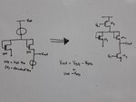
I'm working on subthreshold circuits as part of my project. The image bellow shows Vref as a temperature compensated reference and M3 and M4 as current sources mirrored from a current generator.
37856354_10214515682663753_8785221162901700608_n.jpg

I have simulated the circuit and achieved a temperature compensated Vref. By following the equation,
Vref=Vgs1-Vgs2
Vref=Vth1-Vth2+m*Vt*ln[(W/L)2/(W/L)1]

But Vref is also equal to Vds3. How can I explain that Vref is controlled by M1 and M2 and not a function of the drain-source voltage of M3?
Please correct me if my understanding is wrong. Thanks.

Best regards,
rmanalo27
 

Vref is also equal to Vds3. How can I explain that Vref is controlled by M1 and M2 and not a function of the drain-source voltage of M3?

In schematic simulation - depending on your tool, e.g. SPECTRE - you can just declare the first equation to get Vref.

If this isn't feasible in your simulation tool, you have to put the two node names at the sources in the schematic, e.g. M1s & M2s (instead of Vref for the latter one).

Instead of a difference declaration by equation, you can use a VCVS (from analogLib) to get the difference, like in this example: VCVS_difference-generation.png Call the inputs just like the node names, the output Vref. Then you can name the drain-source voltage of M3 Vref.
 

How is it temperature compensated? I don't get it. Vt is proportional to absolute temperature, and the biasing current is not described here. Compensated means linear dependency?
 

How can I explain that Vref is controlled by M1 and M2 and not a function of the drain-source voltage of M3?

Thinking twice, you have to prove the 2 equations in your above image, in fact by simulation over supply voltage and temperature changes.
 
Thinking twice, you have to prove the 2 equations in your above image, in fact by simulation over supply voltage and temperature changes.

I did simulate the circuit. Over a temperature range of -25 to 100 (above 100 Vref severely degrades due to junction leakages) and swept from Vdd 0.6 to 1.8.

Vref.JPG

But I guess what I really mean is that if the Vds of M3 has any contribution to Vref (or if the value of vds3 is simply vgs1-vgs2).

***Edit:***
By the way. M1 is HVT (Vth~0.7) and M2 is SVT (Vth~0.45)

- - - Updated - - -

How is it temperature compensated? I don't get it. Vt is proportional to absolute temperature, and the biasing current is not described here. Compensated means linear dependency?

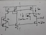
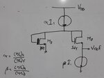
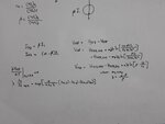
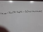
Here is the full schematic (tweaked the original design based from [1])

image1.jpg
image2.jpg
image3.jpg
image 4.jpg

The positive dependence of Vt compensates the negative temperature dependence of Vth.

I got the original circuit from
[1] L. Magnelli, et al, “A 2.6 nW, 0.45 V Temperature-Compensated Subthreshold CMOS Voltage Reference,” IEEE J. Solid-State Circuits, vol. 46, no. 2, pp. 465-474, Feb. 2011.
 

Status
Not open for further replies.

Similar threads

Part and Inventory Search

Welcome to EDABoard.com

Sponsor

Back
Top