boladore
Newbie level 3

- Joined
- May 1, 2011
- Messages
- 4
- Helped
- 0
- Reputation
- 0
- Reaction score
- 0
- Trophy points
- 1,281
- Activity points
- 1,318


Hi there. Sorry for my poor English first.
I have been designing CPW devices, and for the first step, I'm doing simulation for basic CPW structure.
I assigned 100 um to the width of center signal line and from some numerical calculation, 60 um to the gap width for perfect 50 Ohm matching. HFSS showed well matched impedance result.
But since the frequency range I require is from DC to 20 GHz, I did some ADS optimization and found that 120 um is better option for the gap.
So I assigned 120 um to the gap and did HFSS and compared it to the previous design with 60 um gap and it shows that 120 um gap has better insertion and reflection loss. (for S21, from -1.2 to -0.3)
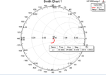
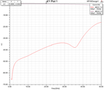
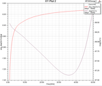
But it also shows impedance mismatch as you can see from the pictures.
So here's the question. As the pictures indicate, the input impedance is away from 50 Ohm(Above 67 Ohm). But as I described before, it shows better S-parameter characteristics.
It makes sense if the result is about characteristic impedance(Z0). But the result is about Zin.
Is there any concept or theory I have missed or the simulation was wrong?
Best regards.