Continue to Site

Welcome to EDAboard.com

Welcome to our site! EDAboard.com is an international Electronics Discussion Forum focused on EDA software, circuits, schematics, books, theory, papers, asic, pld, 8051, DSP, Network, RF, Analog Design, PCB, Service Manuals... and a whole lot more! To participate you need to register. Registration is free. Click here to register now.

What's wrong with my cascade opamp design?

Status
Not open for further replies.

vaka85

Advanced Member level 4
Joined
May 9, 2008
Messages
100
Helped
0
Reputation
0
Reaction score
0
Trophy points
1,296
Activity points
2,112
Hi,

I have to amplify a very small 4 MHz sine signal (about -50 dBm) received from a loopstick antenna (but my problem is the same with a sine input given with a function generator).
Since I'm using a lt1364 (I'm waiting for a more wideband amplifier, now I have that LT and I'm using that one..) which has a gain-bandwidth of 70 MHz, I'm using two stages, each one with an amplification of about 10.

The problem is: if I test the two stages separately, everything is fine, but when I put them together the gain isn't 100 (about) but something around 30...
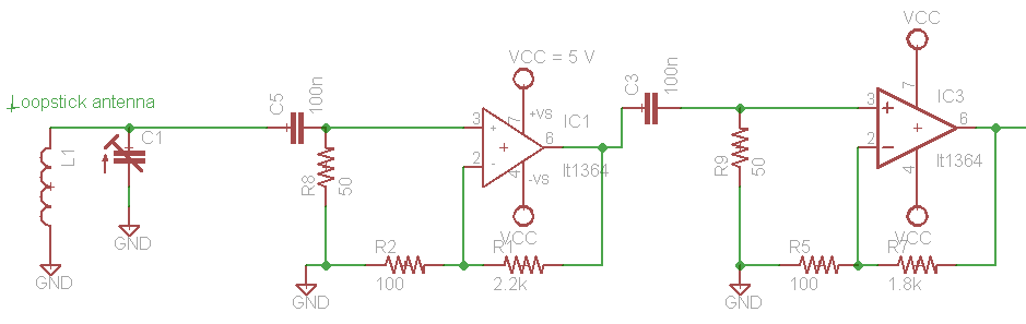
Could you tell me where I'm wrong? here is the schematic:


thank you very much
 

Re: Cascade opamp design

What are the supply voltages in your design?

The 50 Ohm input resistance will be at least an unwanted load to the first stage and considerably reduce it's gain. I also doubt, that you want this kind of load for the antenna.

P.S.: Your circuit will need a solid ground plane to avoid coupling of second stage to the circuit input. Also no supply bypassing is shown in the schematic.
 
Last edited:

Re: Cascade opamp design

they are ± 12V but I can modify them with the power supply unit, if needed..
 

Re: Cascade opamp design

While you cascading the two amplifier circuit, you have to taken care of the matching network. Capacitive matching should be taken into consideration between the two stages for such high frequency circuit.

---------- Post added at 13:43 ---------- Previous post was at 13:41 ----------

I could not able to see your schematic, so i can't able to give suggestion regarding capacitance value changing.
 

Re: Cascade opamp design

@FvM: thank you as always for your advices... At the moment I'm testing the circuit in a breadboard, not very good but is the best I can now... later when the circuit will almost work I'll pass to pcb.. The supply bypass is present, I've not included it in the schematic.
About the 50 ohm resistor. The 2 stages together don't work without it.. I don't know why :(

@muthukumar_ece2004: how to design a capacitive matching network? (sorry for the stupid question)... it should be a filter to isolate only the desidered frequency?
However the schematic is in the first post, maybe you have to login to see it. Here is an external link:
**broken link removed**

thanks
 

Re: Cascade opamp design

+/-12 V should be O.K., +/- 5V is most likely sufficient for low level signals and involves less power dissipation.

As said, I see a major problem with the 50 ohm input resistor. I would increase it to e.g. 5 or 10 kOhm. Coupling between amplifier stages may be an additional issue, depending on the circuit layout. Also don't miss bypass capacitors directly connected to the supply pins and the ground plane. I doubt, that the circuit will work on a breadboard or PCB without solid ground plane or at least a well mashed ground net.

---------- Post added at 10:32 ---------- Previous post was at 10:24 ----------

Capacitive matching should be taken into consideration between the two stages for such high frequency circuit.
Sorry, I don't get the idea. 4 MHz isn't actually a high frequency, still suitable for wideband amplifiers. (I'm operating wideband circuits up to several 100 MHz)
The 2 stages together don't work without it.. I don't know why
Don't work isn't actually a clear observation. Of course, a DC path to the +ve input must be provided, according to the 2 uA bias current. If you possibly observe oscillations without the 50 ohm resistors, this would indicate mainly that the layout is unsuitable for a higher gain. In this case, the circuit may not work without the gain reduction provided by the resistors. Also unwanted feedback from amplifier output to the antenna may be an issue.
 
  • Like
Reactions: vaka85

    vaka85

    Points: 2
    Helpful Answer Positive Rating
Re: Cascade opamp design

I've tried with a potentiometer and several resistor values, but the 50 ohm one appears to be the best one... however I'll try also with the 10Kohm that you've suggested.

So, in your opinion this is a normal behaviour on a breadboard? why it doesn't work at all? but works only "a little"? I thinked that it could work or it couldn't, not a half way :)

Don't work isn't actually a clear observation. Of course, a DC path to the +ve input must be provided, according to the 2 uA bias current. If you possibly observe oscillations without the 50 ohm resistors, this would indicate mainly that the layout is unsuitable for a higher gain. In this case, the circuit may not work without the gain reduction provided by the resistors. Also unwanted feedback from amplifier output to the antenna may be an issue.

Doesn't work: I mean that if you connect the output of the second amplifier to a spectrum analyzer (I'm doing in this way because my scope hasn't so much sensitivity) the 4 MHz component is lost in a very bad spectrum. But if I test stages separately, the 4 MHz component is correctly amplified (only that component, not all the spectrum!).

At this point, as you said, it would be better to pass to a more solid board...
Anyway: what do you mean with " the layout is unsuitable for a higher gain" ?
 

Re: Cascade opamp design

In an electronic circuit each part with its associated value has a certain task.
Therefore my question: What is the task of the 50 ohms resistor at the input of the 2nd stage? Why did you select a value of 50 ohms?
 

Re: Cascade opamp design

you're right, but I have not the complete knowledge of opamp circuits, and I have a very little time to make this circuit works (I know it's not the correct way to do these kind of works..)

I have thinked that maybe there was a problem of impedance matching from the output of the first stage and the input of the second. So, looking in the output impedance graph in the datasheet of lt1364 I've seen that it's around 50 ohm (hard to see the exact value in a logarithmic graph). And so I've put the 50 Ohm resistor...
I've done this right or not?

thanks
 

Re: Cascade opamp design

The amplifier individually working, but while cascading it fails means it must be an impedance mismatching as already told. I think, 100nF and 50E combination not a problem according to frequency response. You may try to connect a variable capacitor (Trimmer) between 3rd pin of second op-amp and ground. At the resonant frequency (4MHz), if the trimmer capacitor may aid to match the resonance of the circuit and provide better amplification.
 

Re: Cascade opamp design

.....................................
So, looking in the output impedance graph in the datasheet of lt1364 I've seen that it's around 50 ohm (hard to see the exact value in a logarithmic graph). And so I've put the 50 Ohm resistor...
I've done this right or not?
thanks

The output impedance of the LT1364 (about 50 ohms) will be drastically reduced due to negative feedback to a value below 1 ohm. Thus, you have pure voltage excitation of the 2nd stage without any necessity to "match" something.
On the other hand, you need a resistor from the positive input of the 2nd opamp to ground (because of dc bias). Because this resistor loads the output of the 1st stage it shouldn't be to small. Therfore, as mentioned by FvM earlier, 5...10 kohms are appropriate.

---------- Post added at 16:21 ---------- Previous post was at 16:17 ----------

...........
At the resonant frequency (4MHz), if the trimmer capacitor may aid to match the resonance of the circuit and provide better amplification.

I don`t understand which resonant effect are you referring to. What is the "resonance of the circuit" ? To me: confusing, sorry.
 

Re: Cascade opamp design

So, looking in the output impedance graph in the datasheet of lt1364 I've seen that it's around 50 ohm (hard to see the exact value in a logarithmic graph). And so I've put the 50 Ohm resistor...
I've done this right or not?
OP (open loop) output impedance surely isn't a subject to impedance matching. In a reasonable designed OP circuit, the closed loop output impedance would be much lower than the open loop value, but in your circuit, there's effectively no loop gain left at 4 MHz. Thus the 50 ohm load will reduce the gain of the driving stage. At the input of the first stage, the 50 ohm load will completely cancel the effect of the tuned antenna, reducing the circuit Q below 1. I can't imagine, that it's wanted this way. Designing the first stage as a high impedance buffer seems the only reasonable option with a tuned antenna.
the 4 MHz component is lost in a very bad spectrum.
I assume, the amplifier chain is oscillating due to uncontrolled feedback of your bredboard design. Even with a good PCB, it may be advisable to use two single OPs instead of a dual type.
The amplifier individually working, but while cascading it fails means it must be an impedance mismatching as already told.
I don't hear substantial knowledge of OP circuits from your words.

The output impedance of the LT1364 (about 50 ohms) will be drastically reduced due to negative feedback to a value below 1 ohm.
It would, with sufficient loop gain. But with 70 MHz GBW there isn't any in this circuit at 4 MHz.
 

Re: Cascade opamp design

ok, so I put the resistor for the dc bias, and the capacitor to remove dc offset.
Now the only problem seems to be the impedance mismatching (if muthukumar_ece2004 is right)..

I really don't understand this issue: if the output of the first has very low resistance, and the input impedance of the second stage is (almost) infinite, how could I match their impedance??

Thank you very much

---------- Post added at 16:38 ---------- Previous post was at 16:33 ----------

sorry FvM we've replied at the same time...

Ok, I'll remove the 50 ohm resistor. I can't understand how the use (or not) of an input buffer is related to the working (or not) behaviour of the 2 stages... If a single stage works even without an input buffer, how can a buffer improve the 2 stage behaviour?
 

Re: Cascade opamp design

In a short, impedance matching (of source and load) can be important in two regards:
- to achieve maximum power transmission in RF circuits, e.g. from a transmitter to an antenna
- when transmission lines are involved. In this situation, you can either implement a source side, load side, or both side impedance matching to supress signal echos by reflected waves. At very high signal frequencies, this technique would be even apllied to short PCB traces.
In your circuit, none of the cases applies.

---------- Post added at 16:49 ---------- Previous post was at 16:43 ----------

I introduced the term high impedance buffer to describe the intended interface to the antenna. I should better say amplifier with high input impedance.
 

Re: Cascade opamp design

but the first amplifier, that now is connect directly to the antenna (LC), has an high impedance input, hasn't it? so here is the input high impedance buffer...

to recap everything you've said:
- impedance matching of source and load isn't very important in my project.
- also impedance matching between the first and the second stage is useless, since the high input impedance of the second stage.
- both amplifiers work if tested one by one.
The problems come when connected together: this problem could be caused by:
- breadboard.
- unexpected behavior caused by uncontrolled feedback from breadboard design.

what else? at this point the only way to prove that the schematic works is making a pcb..

I've forgotten to say that even if I use 2 separated opamp (2 separated chips) I'm using the same supply...
 

Re: Cascade opamp design

I've forgotten to say that even if I use 2 separated opamp (2 separated chips) I'm using the same supply...
That's not a problem as such. Individual bypass capacitors and optional filter inductors in circuits with very high gain can effectively cancel supply crosstalk/feedback.

Above some gain factor, you would wand to enclose the sensitive stages in shielding boxes. You'll find this technique e.g. with most radio or tv receivers.
 

Re: Cascade opamp design

The output impedance of the LT1364 (about 50 ohms) will be drastically reduced due to negative feedback to a value below 1 ohm.

FvM: It would, with sufficient loop gain. But with 70 MHz GBW there isn't any in this circuit at 4 MHz.

A gain of 2.2k/100=22 at 4 Mhz gives a GBW of 88 MHz.
An opamp with GBW=70 Mhz seems not well suited for this task.
 

Re: Cascade opamp design

ok I'll try some modifications and I'll let you know how it works..
thanks!
 

Re: Cascade opamp design

My suggestions: remove C5 and R8 and connect first amp directly to tank. Increase R9 to 1K ; Op-Amps can't drive 50 ohm loads. Oscillation of the composite amp is still likely. You will have to focus on eliminatig feedback
 

Re: Cascade opamp design

it works! :)
(almost...)

here is the final schematic...

**broken link removed**

The total gain it's not 121 but it's not so far...

Many thanks for your help!!
 

Status
Not open for further replies.

Similar threads

Part and Inventory Search

Welcome to EDABoard.com

Sponsor

Back
Top