Continue to Site

Welcome to EDAboard.com

Welcome to our site! EDAboard.com is an international Electronics Discussion Forum focused on EDA software, circuits, schematics, books, theory, papers, asic, pld, 8051, DSP, Network, RF, Analog Design, PCB, Service Manuals... and a whole lot more! To participate you need to register. Registration is free. Click here to register now.

Warning some configuration words not in hex file

Status
Not open for further replies.

Eng.Wad

Member level 2
Joined
Mar 3, 2012
Messages
43
Helped
2
Reputation
4
Reaction score
2
Trophy points
1,288
Activity points
1,551
Hi everyone

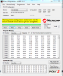
I was trying to write the .hex file into pic18f2550 using pickit 2. before clicking on write" , a warning message appeared in the box:
"Warning some configuration words not in hex file
ensure default values above right are acceptable "

my config is

Code:
#pragma config OSC    = XT  // 4MHz Crystal, (XT oscillator)
#pragma config PBADEN = OFF // PORTB<4:0> pins are configured as digital I/O on Reset)
what shall I configure more ?
if anybody had experienced it before, plz share.

Thanks
 

You maybe using the incorrect/legacy #defines in the configuration register settings.

What compiler and version are you currently using?

Have you looked in the device specific header file for the appropriate #defines?

Also make sure you are not using a zero '0' instead of a letter 'O' used in the word "OFF".

BigDog
 

Thanks for your attention,

these are details of the compiler

Language tool versions: mpasmwin.exe v5.37, mplink.exe v4.37, mcc18.exe v3.36, mplib.exe v4.37

I have no #define lines in my code, I merely have the two lines mentioned above and prototype functions, but I have a linker file with this configuration
Code:
// File: 18f2520_g.lkr
// Generic linker script for the PIC18F2520 processor

#DEFINE _CODEEND _DEBUGCODESTART - 1
#DEFINE _CEND _CODEEND + _DEBUGCODELEN
#DEFINE _DATAEND _DEBUGDATASTART - 1
#DEFINE _DEND _DATAEND + _DEBUGDATALEN

and this is taken from the controller header
Code:
/*-------------------------------------------------------------------------
 * Some useful defines for inline assembly stuff
 *-------------------------------------------------------------------------*/
#define ACCESS 0
#define BANKED 1

/*-------------------------------------------------------------------------
 * Some useful macros for inline assembly stuff
 *-------------------------------------------------------------------------*/
#define Nop()    {_asm nop _endasm}
#define ClrWdt() {_asm clrwdt _endasm}
#define Sleep()  {_asm sleep _endasm}
#define Reset()  {_asm reset _endasm}

#define Rlcf(f,dest,access)  {_asm movlb f rlcf f,dest,access _endasm}
#define Rlncf(f,dest,access) {_asm movlb f rlncf f,dest,access _endasm}
#define Rrcf(f,dest,access)  {_asm movlb f rrcf f,dest,access _endasm}
#define Rrncf(f,dest,access) {_asm movlb f rrncf f,dest,access _endasm}
#define Swapf(f,dest,access) {_asm movlb f swapf f,dest,access _endasm }

/*-------------------------------------------------------------------------
 * A fairly inclusive set of registers to save for interrupts.
 * These are locations which are commonly used by the compiler.
 *-------------------------------------------------------------------------*/
#define INTSAVELOCS TBLPTR, TABLAT, PROD

I made sure of misspelling, they seem correct.
 

Open a DOS/Command window CD to the bin directory of the C18 Compiler and execute the following:

Code:
mcc18.exe -p18f2550 --help-config

The above command will provide a list of all valid configuration bit settings:

Code:
Configuration settings available for processor PIC18F2550

  PLL Prescaler Selection bits:
    PLLDIV = 1          No prescale (4 MHz oscillator input drives PLL
                        directly)
    PLLDIV = 2          Divide by 2 (8 MHz oscillator input)
    PLLDIV = 3          Divide by 3 (12 MHz oscillator input)
    PLLDIV = 4          Divide by 4 (16 MHz oscillator input)
    PLLDIV = 5          Divide by 5 (20 MHz oscillator input)
    PLLDIV = 6          Divide by 6 (24 MHz oscillator input)
    PLLDIV = 10         Divide by 10 (40 MHz oscillator input)
    PLLDIV = 12         Divide by 12 (48 MHz oscillator input)

  System Clock Postscaler Selection bits:
    CPUDIV = OSC1_PLL2  [Primary Oscillator Src: /1][96 MHz PLL Src: /2]
    CPUDIV = OSC2_PLL3  [Primary Oscillator Src: /2][96 MHz PLL Src: /3]
    CPUDIV = OSC3_PLL4  [Primary Oscillator Src: /3][96 MHz PLL Src: /4]
    CPUDIV = OSC4_PLL6  [Primary Oscillator Src: /4][96 MHz PLL Src: /6]

  USB Clock Selection bit (used in Full-Speed USB mode only; UCFG:FSEN = 1):
    USBDIV = 1          USB clock source comes directly from the primary
                        oscillator block with no postscale
    USBDIV = 2          USB clock source comes from the 96 MHz PLL divided by 2

  Oscillator Selection bits:
    FOSC = XT_XT        XT oscillator (XT)
    FOSC = XTPLL_XT     XT oscillator, PLL enabled (XTPLL)
    FOSC = ECIO_EC      EC oscillator, port function on RA6 (ECIO)
    FOSC = EC_EC        EC oscillator, CLKO function on RA6 (EC)
    FOSC = ECPLLIO_EC   EC oscillator, PLL enabled, port function on RA6
                        (ECPIO)
    FOSC = ECPLL_EC     EC oscillator, PLL enabled, CLKO function on RA6
                        (ECPLL)
    FOSC = INTOSCIO_EC  Internal oscillator, port function on RA6, EC used by
                        USB (INTIO)
    FOSC = INTOSC_EC    Internal oscillator, CLKO function on RA6, EC used by
                        USB (INTCKO)
    FOSC = INTOSC_XT    Internal oscillator, XT used by USB (INTXT)
    FOSC = INTOSC_HS    Internal oscillator, HS oscillator used by USB (INTHS)
    FOSC = HS           HS oscillator (HS)
    FOSC = HSPLL_HS     HS oscillator, PLL enabled (HSPLL)

  Fail-Safe Clock Monitor Enable bit:
    FCMEN = OFF         Fail-Safe Clock Monitor disabled
    FCMEN = ON          Fail-Safe Clock Monitor enabled

  Internal/External Oscillator Switchover bit:
    IESO = OFF          Oscillator Switchover mode disabled
    IESO = ON           Oscillator Switchover mode enabled

  Power-up Timer Enable bit:
    PWRT = ON           PWRT enabled
    PWRT = OFF          PWRT disabled

  Brown-out Reset Enable bits:
    BOR = OFF           Brown-out Reset disabled in hardware and software
    BOR = SOFT          Brown-out Reset enabled and controlled by software
                        (SBOREN is enabled)
    BOR = ON_ACTIVE     Brown-out Reset enabled in hardware only and disabled
                        in Sleep mode (SBOREN is disabled)
    BOR = ON            Brown-out Reset enabled in hardware only (SBOREN is
                        disabled)

  Brown-out Reset Voltage bits:
    BORV = 0            Maximum setting
    BORV = 1
    BORV = 2
    BORV = 3            Minimum setting

  USB Voltage Regulator Enable bit:
    VREGEN = OFF        USB voltage regulator disabled
    VREGEN = ON         USB voltage regulator enabled

  Watchdog Timer Enable bit:
    WDT = OFF           WDT disabled (control is placed on the SWDTEN bit)
    WDT = ON            WDT enabled

  Watchdog Timer Postscale Select bits:
    WDTPS = 1           1:1
    WDTPS = 2           1:2
    WDTPS = 4           1:4
    WDTPS = 8           1:8
    WDTPS = 16          1:16
    WDTPS = 32          1:32
    WDTPS = 64          1:64
    WDTPS = 128         1:128
    WDTPS = 256         1:256
    WDTPS = 512         1:512
    WDTPS = 1024        1:1024
    WDTPS = 2048        1:2048
    WDTPS = 4096        1:4096
    WDTPS = 8192        1:8192
    WDTPS = 16384       1:16384
    WDTPS = 32768       1:32768

  CCP2 MUX bit:
    CCP2MX = OFF        CCP2 input/output is multiplexed with RB3
    CCP2MX = ON         CCP2 input/output is multiplexed with RC1

  PORTB A/D Enable bit:
    PBADEN = OFF        PORTB<4:0> pins are configured as digital I/O on Reset
    PBADEN = ON         PORTB<4:0> pins are configured as analog input
                        channels on Reset

  Low-Power Timer 1 Oscillator Enable bit:
    LPT1OSC = OFF       Timer1 configured for higher power operation
    LPT1OSC = ON        Timer1 configured for low-power operation

  MCLR Pin Enable bit:
    MCLRE = OFF         RE3 input pin enabled; MCLR pin disabled
    MCLRE = ON          MCLR pin enabled; RE3 input pin disabled

  Stack Full/Underflow Reset Enable bit:
    STVREN = OFF        Stack full/underflow will not cause Reset
    STVREN = ON         Stack full/underflow will cause Reset

  Single-Supply ICSP Enable bit:
    LVP = OFF           Single-Supply ICSP disabled
    LVP = ON            Single-Supply ICSP enabled

  Extended Instruction Set Enable bit:
    XINST = OFF         Instruction set extension and Indexed Addressing mode
                        disabled (Legacy mode)
    XINST = ON          Instruction set extension and Indexed Addressing mode
                        enabled

  Background Debugger Enable bit:
    DEBUG = ON          Background debugger enabled, RB6 and RB7 are dedicated
                        to In-Circuit Debug
    DEBUG = OFF         Background debugger disabled, RB6 and RB7 configured
                        as general purpose I/O pins

  Code Protection bit:
    CP0 = ON            Block 0 (000800-001FFFh) is code-protected
    CP0 = OFF           Block 0 (000800-001FFFh) is not code-protected

  Code Protection bit:
    CP1 = ON            Block 1 (002000-003FFFh) is code-protected
    CP1 = OFF           Block 1 (002000-003FFFh) is not code-protected

  Code Protection bit:
    CP2 = ON            Block 2 (004000-005FFFh) is code-protected
    CP2 = OFF           Block 2 (004000-005FFFh) is not code-protected

  Code Protection bit:
    CP3 = ON            Block 3 (006000-007FFFh) is code-protected
    CP3 = OFF           Block 3 (006000-007FFFh) is not code-protected

  Boot Block Code Protection bit:
    CPB = ON            Boot block (000000-0007FFh) is code-protected
    CPB = OFF           Boot block (000000-0007FFh) is not code-protected

  Data EEPROM Code Protection bit:
    CPD = ON            Data EEPROM is code-protected
    CPD = OFF           Data EEPROM is not code-protected

  Write Protection bit:
    WRT0 = ON           Block 0 (000800-001FFFh) is write-protected
    WRT0 = OFF          Block 0 (000800-001FFFh) is not write-protected

  Write Protection bit:
    WRT1 = ON           Block 1 (002000-003FFFh) is write-protected
    WRT1 = OFF          Block 1 (002000-003FFFh) is not write-protected

  Write Protection bit:
    WRT2 = ON           Block 2 (004000-005FFFh) is write-protected
    WRT2 = OFF          Block 2 (004000-005FFFh) is not write-protected

  Write Protection bit:
    WRT3 = ON           Block 3 (006000-007FFFh) is write-protected
    WRT3 = OFF          Block 3 (006000-007FFFh) is not write-protected

  Configuration Register Write Protection bit:
    WRTC = ON           Configuration registers (300000-3000FFh) are
                        write-protected
    WRTC = OFF          Configuration registers (300000-3000FFh) are not
                        write-protected

  Boot Block Write Protection bit:
    WRTB = ON           Boot block (000000-0007FFh) is write-protected
    WRTB = OFF          Boot block (000000-0007FFh) is not write-protected

  Data EEPROM Write Protection bit:
    WRTD = ON           Data EEPROM is write-protected
    WRTD = OFF          Data EEPROM is not write-protected

  Table Read Protection bit:
    EBTR0 = ON          Block 0 (000800-001FFFh) is protected from table reads
                        executed in other blocks
    EBTR0 = OFF         Block 0 (000800-001FFFh) is not protected from table
                        reads executed in other blocks

  Table Read Protection bit:
    EBTR1 = ON          Block 1 (002000-003FFFh) is protected from table reads
                        executed in other blocks
    EBTR1 = OFF         Block 1 (002000-003FFFh) is not protected from table
                        reads executed in other blocks

  Table Read Protection bit:
    EBTR2 = ON          Block 2 (004000-005FFFh) is protected from table reads
                        executed in other blocks
    EBTR2 = OFF         Block 2 (004000-005FFFh) is not protected from table
                        reads executed in other blocks

  Table Read Protection bit:
    EBTR3 = ON          Block 3 (006000-007FFFh) is protected from table reads
                        executed in other blocks
    EBTR3 = OFF         Block 3 (006000-007FFFh) is not protected from table
                        reads executed in other blocks

  Boot Block Table Read Protection bit:
    EBTRB = ON          Boot block (000000-0007FFh) is protected from table
                        reads executed in other blocks
    EBTRB = OFF         Boot block (000000-0007FFh) is not protected from
                        table reads executed in other blocks

The following is most likely the source of the error message.

The valid Oscillator setting for a 4MHz Crystal should be:

Code:
 #pragma config FOSC = XT_XT

or

Code:
 #pragma config  FOSC = HS

Rather than:

Code:
#pragma config OSC    = XT  // 4MHz Crystal, (XT oscillator)


BigDog
 

After reviewing your initial post, the compiler message you received:

"Warning some configuration words not in hex file
ensure default values above right are acceptable "

Is simply warning you that the configuration register settings which you have not explicitly set will be set their default values.

To ensure the configuration register settings are correct, you can explicitly set all the remaining values:

Code:
Configuration settings available for processor PIC18F2520

  Oscillator Selection bits:
    OSC = LP            LP oscillator
    OSC = XT            XT oscillator
    OSC = HS            HS oscillator
    OSC = RC            External RC oscillator, CLKO function on RA6
    OSC = EC            EC oscillator, CLKO function on RA6
    OSC = ECIO6         EC oscillator, port function on RA6
    OSC = HSPLL         HS oscillator, PLL enabled (Clock Frequency = 4 x
                        FOSC1)
    OSC = RCIO6         External RC oscillator, port function on RA6
    OSC = INTIO67       Internal oscillator block, port function on RA6 and RA7
    OSC = INTIO7        Internal oscillator block, CLKO function on RA6, port
                        function on RA7

  Fail-Safe Clock Monitor Enable bit:
    FCMEN = OFF         Fail-Safe Clock Monitor disabled
    FCMEN = ON          Fail-Safe Clock Monitor enabled

  Internal/External Oscillator Switchover bit:
    IESO = OFF          Oscillator Switchover mode disabled
    IESO = ON           Oscillator Switchover mode enabled

  Power-up Timer Enable bit:
    PWRT = ON           PWRT enabled
    PWRT = OFF          PWRT disabled

  Brown-out Reset Enable bits:
    BOREN = OFF         Brown-out Reset disabled in hardware and software
    BOREN = ON          Brown-out Reset enabled and controlled by software
                        (SBOREN is enabled)
    BOREN = NOSLP       Brown-out Reset enabled in hardware only and disabled
                        in Sleep mode (SBOREN is disabled)
    BOREN = SBORDIS     Brown-out Reset enabled in hardware only (SBOREN is
                        disabled)

  Brown Out Reset Voltage bits:
    BORV = 0            Maximum setting
    BORV = 1
    BORV = 2
    BORV = 3            Minimum setting

  Watchdog Timer Enable bit:
    WDT = OFF           WDT disabled (control is placed on the SWDTEN bit)
    WDT = ON            WDT enabled

  Watchdog Timer Postscale Select bits:
    WDTPS = 1           1:1
    WDTPS = 2           1:2
    WDTPS = 4           1:4
    WDTPS = 8           1:8
    WDTPS = 16          1:16
    WDTPS = 32          1:32
    WDTPS = 64          1:64
    WDTPS = 128         1:128
    WDTPS = 256         1:256
    WDTPS = 512         1:512
    WDTPS = 1024        1:1024
    WDTPS = 2048        1:2048
    WDTPS = 4096        1:4096
    WDTPS = 8192        1:8192
    WDTPS = 16384       1:16384
    WDTPS = 32768       1:32768

  CCP2 MUX bit:
    CCP2MX = PORTBE     CCP2 input/output is multiplexed with RB3
    CCP2MX = PORTC      CCP2 input/output is multiplexed with RC1

  PORTB A/D Enable bit:
    PBADEN = OFF        PORTB<4:0> pins are configured as digital I/O on Reset
    PBADEN = ON         PORTB<4:0> pins are configured as analog input
                        channels on Reset

  Low-Power Timer1 Oscillator Enable bit:
    LPT1OSC = OFF       Timer1 configured for higher power operation
    LPT1OSC = ON        Timer1 configured for low-power operation

  MCLR Pin Enable bit:
    MCLRE = OFF         RE3 input pin enabled; MCLR disabled
    MCLRE = ON          MCLR pin enabled; RE3 input pin disabled

  Stack Full/Underflow Reset Enable bit:
    STVREN = OFF        Stack full/underflow will not cause Reset
    STVREN = ON         Stack full/underflow will cause Reset

  Single-Supply ICSP Enable bit:
    LVP = OFF           Single-Supply ICSP disabled
    LVP = ON            Single-Supply ICSP enabled

  Extended Instruction Set Enable bit:
    XINST = OFF         Instruction set extension and Indexed Addressing mode
                        disabled (Legacy mode)
    XINST = ON          Instruction set extension and Indexed Addressing mode
                        enabled

  Background Debugger Enable bit:
    DEBUG = ON          Background debugger enabled, RB6 and RB7 are dedicated
                        to In-Circuit Debug
    DEBUG = OFF         Background debugger disabled, RB6 and RB7 configured
                        as general purpose I/O pins

  Code Protection bit:
    CP0 = ON            Block 0 (000800-001FFFh) code-protected
    CP0 = OFF           Block 0 (000800-001FFFh) not code-protected

  Code Protection bit:
    CP1 = ON            Block 1 (002000-003FFFh) code-protected
    CP1 = OFF           Block 1 (002000-003FFFh) not code-protected

  Code Protection bit:
    CP2 = ON            Block 2 (004000-005FFFh) code-protected
    CP2 = OFF           Block 2 (004000-005FFFh) not code-protected

  Code Protection bit:
    CP3 = ON            Block 3 (006000-007FFFh) code-protected
    CP3 = OFF           Block 3 (006000-007FFFh) not code-protected

  Boot Block Code Protection bit:
    CPB = ON            Boot block (000000-0007FFh) code-protected
    CPB = OFF           Boot block (000000-0007FFh) not code-protected

  Data EEPROM Code Protection bit:
    CPD = ON            Data EEPROM code-protected
    CPD = OFF           Data EEPROM not code-protected

  Write Protection bit:
    WRT0 = ON           Block 0 (000800-001FFFh) write-protected
    WRT0 = OFF          Block 0 (000800-001FFFh) not write-protected

  Write Protection bit:
    WRT1 = ON           Block 1 (002000-003FFFh) write-protected
    WRT1 = OFF          Block 1 (002000-003FFFh) not write-protected

  Write Protection bit:
    WRT2 = ON           Block 2 (004000-005FFFh) write-protected
    WRT2 = OFF          Block 2 (004000-005FFFh) not write-protected

  Write Protection bit:
    WRT3 = ON           Block 3 (006000-007FFFh) write-protected
    WRT3 = OFF          Block 3 (006000-007FFFh) not write-protected

  Configuration Register Write Protection bit:
    WRTC = ON           Configuration registers (300000-3000FFh)
                        write-protected
    WRTC = OFF          Configuration registers (300000-3000FFh) not
                        write-protected

  Boot Block Write Protection bit:
    WRTB = ON           Boot block (000000-0007FFh) write-protected
    WRTB = OFF          Boot block (000000-0007FFh) not write-protected

  Data EEPROM Write Protection bit:
    WRTD = ON           Data EEPROM write-protected
    WRTD = OFF          Data EEPROM not write-protected

  Table Read Protection bit:
    EBTR0 = ON          Block 0 (000800-001FFFh) protected from table reads
                        executed in other blocks
    EBTR0 = OFF         Block 0 (000800-001FFFh) not protected from table
                        reads executed in other blocks

  Table Read Protection bit:
    EBTR1 = ON          Block 1 (002000-003FFFh) protected from table reads
                        executed in other blocks
    EBTR1 = OFF         Block 1 (002000-003FFFh) not protected from table
                        reads executed in other blocks

  Table Read Protection bit:
    EBTR2 = ON          Block 2 (004000-005FFFh) protected from table reads
                        executed in other blocks
    EBTR2 = OFF         Block 2 (004000-005FFFh) not protected from table
                        reads executed in other blocks

  Table Read Protection bit:
    EBTR3 = ON          Block 3 (006000-007FFFh) protected from table reads
                        executed in other blocks
    EBTR3 = OFF         Block 3 (006000-007FFFh) not protected from table
                        reads executed in other blocks

  Boot Block Table Read Protection bit:
    EBTRB = ON          Boot block (000000-0007FFh) protected from table reads
                        executed in other blocks
    EBTRB = OFF         Boot block (000000-0007FFh) not protected from table
                        reads executed in other blocks

I normally use a template header file with all the configuration register settings preset in #pragma config statements and simply change those settings relevant to the current project.

BigDog
 

This what I was talking about, what could be the problem?


warning.PNG
 

I'll give short description of my code up to this moment.

I'm controlling 6 leds using push ON/OFF buttons, my OSC is 4MHz. the code was developed using c18. what configurations could be made for it?
 

Any hints guys, got stuck at this point :???:
 

Status
Not open for further replies.

Similar threads

Part and Inventory Search

Welcome to EDABoard.com

Sponsor

Back
Top